NextPCB Capabilities
Printed Circuit Boards
NextPCB Capabilities
Printed Circuit Boards
 PCB Assembly
 Layer Buildup
 SMD-Stencils
 PCB Design-Aid & Layout
 Mechanics
 Quality
 Drills & Throughplating
 Factory & Certificate
 PCB Assembly Factory Show
Certificate
PCB Assembly Factory Show
Certificate
Support Team
Feedback:
support@nextpcb.com


Introduction
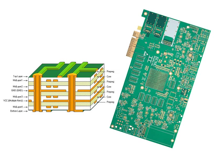
Due to the increasing density of chip packaging, the interconnections have also become more compact. This brings a significant issue: single layer PCBs or double layer PCBs are no longer sufficient, leading to the adoption of multilayer PCBs. A multilayer PCB is a circuit board made by stacking two or more layers of circuits together, with reliable pre-defined interconnections between them. To better understand the necessity and complexity of multilayer PCBs (MPCBs), it is essential to first analyze the foundational limitations of simpler structures and the advanced engineering principles required to overcome them.
Table of Contents
The rapid advancement in semiconductor technology, particularly the shift toward high-I/O count components utilizing Ball Grid Array (BGA) and Fine-Pitch BGA (FBGA) packaging, has made the use of single- and double-layer PCBs obsolete for almost all high-performance designs. The fundamental limitation of 2-layer PCBs (DLPs) is their inability to provide continuous, solid reference planes (Ground and Power) while simultaneously accommodating high routing density. In a DLP, traces must constantly jump between the two outer layers using through-hole vias, severely fragmenting the necessary reference return paths. This fragmentation introduces significant signal integrity (SI) issues, including increased crosstalk, substantial electromagnetic interference (EMI), and generally poor electromagnetic compatibility (EMC).
> Recommend reading: Best 6-Layer PCB Stackups for Signal Integrity & Impedance Control
Modern semiconductor packaging, specifically high-I/O Ball Grid Array (BGA) components, often require extreme routing density, with pitch dimensions routinely less than 0.5mm. Routing the escape patterns beneath these components demands a high density of vertical interconnections that cannot be achieved efficiently using only simple through-holes. MPCBs provide the structural framework needed to transition routing from a planar (2D) approach to a stacked (3D) engineering solution.
A multilayer PCB is a circuit board made by stacking two or more layers of circuits together, with reliable pre-defined interconnections between them. Crucially, an MPCB is a controlled stackup of conductive layers (copper foil) separated by prepreg (B-stage resin) and cores (C-stage laminate) that are laminated together under intense heat and pressure to form a solid, monolithic structure. The layers are typically designated for specific functions: Signal (S), Ground (GND), and Power (PWR), allowing for intentional, high-performance electrical routing.
The foundation of robust MPCB design begins at the 4-layer configuration. The four-layer structure (typically Signal, Ground, Power, Signal) is the minimum required to establish the necessary continuous reference planes for controlled impedance routing. This architecture immediately addresses fundamental SI concerns by dedicating two interior layers to solid, low-inductance return paths. Without these solid reference layers, high-speed signals cannot propagate reliably because the electromagnetic field of the signal trace needs a constant, adjacent return path to minimize loop inductance and prevent impedance discontinuities.
As design requirements exceed the capacity of a four-layer board, layer counts escalate significantly. Applications in complex computation, high-speed networking, and large data center infrastructure often necessitate extremely complex stackups.
High-end server motherboards and telecom backplanes routinely require 8, 12, 16, or more layers, pushing fabrication complexity to its limit. A fabricator's ability to handle these complex structures is a direct indication of their experience and expertise. For instance, NextPCB officially supports up to 32+ Maximum Layers, a specification that demonstrates top-tier capability in managing extreme stackup complexity, including high layer count sequential lamination, monumental thermal management, and achieving perfect layer registration across numerous manufacturing cycles.
The technical infrastructure required to successfully manufacture 32-layer boards is a strong signal of Authoritativeness within the high-reliability manufacturing sector, as these boards are generally utilized in mission-critical applications such as defense systems or central networking hubs.
> Recommend reading: Fundamentals of PCB Thermal Design | NextPCB
The longevity and performance of a multilayer PCB are fundamentally determined by the base materials used. Mismatched or improperly specified materials are the leading cause of field failures, thermal fatigue, and signal degradation.
The selection of base materials (laminates) is the most critical decision impacting both electrical performance and mechanical reliability. The industry relies on standardized frameworks to ensure quality and compliance. IPC-4101 provides the definitive specification for rigid and multilayer PCB base substrates, ensuring that cores and prepregs meet standardized parameters for quality, thermal stability, and electrical performance.
By utilizing IPC classification numbers, designers can communicate precise and unambiguous requirements to manufacturers, aligning material characteristics—such as thickness uniformity, resin flow, and thermal expansion—with the final application needs.
Tg defines the temperature ceiling for the material's structural integrity. It is the point at which the polymer matrix transitions from a rigid, glassy state to a soft, rubbery state. Operating a PCB above its Tg leads to dimensional instability, which compromises the integrity of plated through-holes (PTHs) and can result in delamination.
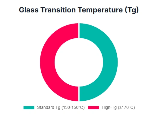
The Significance of High-Tg Laminates
For high-power industrial, automotive, or aerospace applications where internal operating temperatures are elevated, materials with a Tg above 170°C (e.g., 170°C – 180°C) are mandatory to prevent delamination and PTH failure during prolonged use. Standard FR-4 typically has a Tg around 130°C. The capacity to procure and process higher performance materials is a measure of fabricator capability. The ability of NextPCB to support high Tg materials up to 170°C – 180°C demonstrates capability for high-reliability manufacturing required in rigorous environments.
Td is the temperature at which the material chemically decomposes. This measure is crucial for determining safe assembly and rework temperatures. If the board is subjected to temperatures exceeding its Td during assembly (e.g., reflow soldering), the laminate permanently degrades, resulting in catastrophic failure.
Electrical Criticality: Dielectric Constant (Dk) and Dissipation Factor (Df)
For high-speed digital and RF designs, electrical properties supersede thermal or mechanical ones. The dielectric constant and dissipation factor dictate how fast signals travel and how much energy is lost.
The Dielectric Constant (Dk or εr) directly influences the speed of signal propagation and the characteristic impedance (Z0). Signal velocity is inversely proportional to the square root of Dk. For high-frequency applications (typically above 1 GHz), lower Dk values (e.g., 3.0 to 3.5) are necessary to minimize signal delay and maintain stable impedance. Higher Dk materials slow the signal and introduce more latency.
The Dissipation Factor (Df) represents energy lost as heat, which translates directly to signal attenuation. This loss is particularly problematic at high frequencies. Low Df materials are essential for high-speed digital and RF applications where signal loss (insertion loss) must be minimized. For cutting-edge applications, such as 5G infrastructure, materials with Df values as low as 0.0015 are often specified to ensure minimal energy attenuation and high signal quality.
High-speed and RF laminates, such as Megtron 6 or RO4350B, which exhibit very low Dk and Df, fall under the specific guidelines of IPC-4103. This designation signals their suitability for applications demanding precise electrical characteristics at extreme frequencies. The use of specialized materials under IPC-4103 confirms that a design is constrained by electrical physics rather than mere density.
The Coefficient of Thermal Expansion (CTE) measures how much a material expands when heated. High CTE, particularly in the Z-axis (thickness), subjects the plated copper barrels of vias to enormous stress during thermal cycling (e.g., soldering or operation). Excessive Z-axis expansion can lead directly to barrel cracking and connectivity failures.
IPC-4101 defines CTE limits to match materials with components and reduce stress. In a complex MPCB stackup (8 layers & 8+ layers), every layer adds thermal stress. Using low Z-CTE materials, often correlated with high-Tg properties (e.g., FR-4 4101/26, with Z-CTE of 70–90 ppm/°C), minimizes the expansion differential between the laminate and the copper plating, directly improving the long-term reliability of internal interconnections, which is paramount for long-term Trustworthiness in technical applications.
Layer separation, known as delamination, is a primary mechanical failure mode caused by poor bonding or severe thermal stress. IPC-4101 explicitly specifies prepreg resin content and flow properties to ensure robust adhesion during the lamination process.
The following table summarizes the material specifications critical for MPCB design:
| Material Example | IPC Standard | Tg (°C) | Dk @ 10GHz (Approx.) | Df @ 10GHz (Approx.) | Z-CTE (ppm/°C) | Primary Use Case |
|---|---|---|---|---|---|---|
| FR-4 (Standard) | IPC-4101/21 | ~130 | 4.3 | 0.02 | 180 | Consumer Electronics |
| FR-4 (High Tg) | IPC-4101/26 | ~180 | 4.2 | 0.015 | 70–90 | Industrial/Automotive |
| Megtron 6 | IPC-4103 | >200 | 3.6 | 0.0022 | ~60 | 100G Backplane/Routers |
| RO4350B | IPC-4103 | ~280 | 3.48 | 0.0037 | ~40 | 5G RF Modules, Radar |
The cost of moving from commodity FR-4 to specialized materials (IPC-4103 certified) represents the steepest cost trade-off in MPCB manufacturing. This is evident in pricing models where even a moderate increase in thermal requirement, such as specifying Tg from 130°C to 170°C, can result in a substantial cost jump. This cost increase is driven not only by the raw material expense but also by the lower production yield and increased inspection complexity associated with handling and processing these higher-performance laminates.
>>> Related Advanced PCB Materials & Structures
Engineering references aligned with high-speed signal integrity, HDI routing, and thermal reliability.
For data rates exceeding approximately 50 MHz, traces must be treated as transmission lines, where the characteristic impedance (Z0) must be controlled and matched to the system components to prevent signal reflections and ensure data integrity.
> Recommend reading: Understanding Impedance Control in PCBs
Controlled Impedance refers to designing traces such that their characteristic impedance (Z0) matches the IC driver/receiver specifications (typically 50Ω for single-ended traces or 100Ω for differential pairs). Any impedance mismatch causes reflections, leading to jitter, signal distortion, and potential functional failure. The characteristic impedance calculation for a trace is governed by four primary variables: the trace geometry (Width w and Thickness t), the dielectric height (h), and the material's relative dielectric constant (εr or Dk). Precise control over these variables is mandatory for MPCB reliability.
A microstrip line is created when a signal trace is routed on an outer layer (L1 or LN), referenced to the nearest inner ground or power plane. The dominant mode of propagation in microstrip is Quasi-TEM (Transverse Electromagnetic). Because the electromagnetic field travels partly in the dielectric substrate and partly in the air above the trace, the effective dielectric constant is frequency-dependent. This dependence results in frequency-dependent phase velocity and characteristic impedance (Z0), posing challenges for ultra-high-speed signals.
Microstrip traces are susceptible to higher dielectric loss and conductor loss due to less complete shielding. Furthermore, microstrip acts partially as an antenna, leading to higher electromagnetic emissions and increased crosstalk sensitivity compared to internal routing options. Strategies to mitigate these issues include using wider traces to reduce ohmic (conduction) loss and minimizing the dielectric height (h).
A stripline configuration is achieved when a signal trace is routed entirely on an internal layer, completely sandwiched symmetrically between two solid reference planes (e.g., Ground-Signal-Ground). Stripline geometry supports a pure TEM mode, meaning the electromagnetic field is contained almost entirely within the dielectric material. This containment results in highly predictable phase velocity and characteristic impedance, making Z0 stable and largely independent of frequency variations up to extremely high speeds.
The presence of dual, solid ground planes provides superior shielding, significantly reducing electromagnetic emissions and minimizing crosstalk compared to microstrip routing. This superior electrical isolation makes stripline the preferred architecture for high-speed differential pairs and sensitive analog signals. While superior electrically, stripline traces still incur losses due to conductor conductivity, magnetic resonances, and dielectric damping effects. The decision to route critical signals as stripline inherently increases cost by requiring a minimum four-layer stackup (or more complex balanced stacks) and demanding tighter thickness tolerances on the prepreg layers that define the stripline gap. This confirms that superior electrical performance is a factor that must be explicitly planned and budgeted for.
| Microstrip (Outer) | Stripline (Inner) | |
|---|---|---|
| Location | Outer Layer (Signal over one Ground Plane) | Inner Layer (Signal between Two Ground Planes) |
| Propagation Mode | Quasi-TEM (Frequency-Dependent Z0) | Pure TEM (Stable Z0) |
| EMI/Crosstalk | Higher Emissions/Sensitivity (Unshielded) | Lower Emissions/Sensitivity (Shielded) |
| Manufacturing Cost | Generally lower (simpler reference) | Higher (requires dual reference planes) |
| Optimal Use Case | Non-critical nets, low-to-mid speed | High-speed differential pairs, sensitive analog signals |
Achieving the target impedance requires highly precise control over fabrication tolerances (trace width, copper thickness) and accurate knowledge of material properties (Dk). Impedance calculation relies entirely on the accuracy of the variables w, t, h, and εr. If a manufacturer's actual dielectric thickness (h) or copper thickness (t) deviates from the stackup plan, the resulting Z0 will be incorrect, leading to performance issues.
Designers must use complex field solvers, often integrated into advanced PCB CAD software (such as those found in Altium Designer), to model the desired trace geometry for a target impedance. These tools require accurate dielectric constant (Dk) data from the fabricator to generate precise results. The fabricator must adhere to extremely tight dimensional specifications, particularly regarding line width and spacing. NextPCB's published minimum trace width/spacing capability of 3mil is critical for achieving high-density, controlled impedance routing required for advanced digital designs. Furthermore, NextPCB's capability to handle custom copper weights up to 6oz or custom options highlights their control over the trace thickness variable (t), providing engineers with the precise parameters needed for accurate impedance simulation and design.
If you want to better meet your own design stackup structure and impedance requirements, you can use NextPCB's online stackup and impedance calculator.
Online Stackup and Impedance Calculator
The drive toward miniaturization in electronics mandates the use of High-Density Interconnect (HDI) technology, which utilizes smaller features and more complex vertical interconnections than standard MPCBs.
HDI refers to PCBs that utilize microvias and extremely fine lines/spaces (3mil or less) to achieve significantly higher component density than traditional MPCBs. HDI technology is mandatory for applications requiring compact footprints, such as smartphones, wearable devices, and advanced computing modules that utilize fine-pitch BGA packages. Standard through-hole vias have large annular rings that consume valuable routing real estate. HDI necessitates highly targeted, smaller vertical connections: blind and buried vias.
Blind vias connect an outer layer to one or more internal layers. They are "blind" because they stop at an internal layer and do not pass through the entire board thickness.
Buried vias connect only internal layers and are completely "buried" within the board structure. They are invisible from the outer surfaces.
The manufacturing of both blind and buried vias requires complex processing steps, including sequential lamination and depth-controlled drilling (either mechanical or laser), substantially increasing fabrication cost and time compared to simple through-holes.
Microvias are defined as blind or buried vias with a finished diameter typically less than or equal to 0.15 mm. They are commonly formed by laser drilling due to their small size and the necessity for precise depth control. Microvias are essential for escaping ultra-fine pitch components, such as 0.3 mm pitch BGA components, enabling the dense routing required beneath the IC package without compromising trace integrity or clearance.
High Aspect Ratio (AR), the ratio of the hole depth to its diameter, microvias present major plating challenges. Achieving uniform and reliable copper plating throughout the barrel of a deep, narrow microvia requires advanced laser drilling and specialized plating techniques. Fabricators must balance the trade-offs between staggering or stacking these microvias to maximize routing density while ensuring manufacturability and high reliability.
Via-in-Pad (VIP) technology involves placing a microvia directly within the surface mount pad of a component, maximizing routing density and minimizing trace lengths beneath high-density packages. While traditional VIP for mechanical vias often required costly epoxy filling, modern HDI microvias (uvias) are typically fabricated using wrap plating (plated solid). With HDI uvias, the microvia is plated solid and does not require a separate, expensive epoxy filling step for most applications. This has made solid-plated microvia-in-pad the preferred and often most cost-effective HDI connection method for advanced designs, despite the initial complexity. NextPCB explicitly offers Via in Pad capability, supporting this critical HDI manufacturing technique.
Manufacturing complex HDI boards necessitates the process of sequential lamination. Sequential lamination involves repeating the lamination, drilling, and plating steps multiple times. For example, a high-end 4-N-4 HDI board (four microvia layers on each side of the core) requires multiple cycles: the core is laminated and drilled, then another layer of prepreg/foil is added, laminated, and laser-drilled for the next microvia layer, and so on.
The multiple lamination cycles and the precise drilling required for microvias and other features significantly increase production time, extend the overall lead time, and raise the total fabrication cost compared to traditional single-cycle lamination methods. However, the structural complexity afforded by this process offers essential benefits. Sequential lamination allows designers to create highly complex multilayer structures tailored to specific applications, such as 20-layer boards for data centers.
By packing more functionality into fewer total layers, the process can sometimes reduce the overall board thickness and optimize layer count. Crucially, the process demands stringent alignment accuracy; each successive layer must be perfectly aligned during lamination to prevent misalignment of vias and traces, which would result in electrical failure. A high quality rate (e.g., NextPCB's 99.8% quality rate) in sequential lamination is a profound signal of manufacturing control over this highly complex, multi-stage alignment process.
Theoretical design compliance must be quantitatively verified during production. Because manufacturing variations—such as minor deviations in etching consistency (affecting trace width) or variations in lamination pressure (affecting dielectric height)—can cause the actual impedance to deviate from the calculated design impedance, rigorous, quantifiable testing is essential to confirm Trustworthiness and production reliability.
The performance of high-speed MPCBs is dependent on maintaining consistent characteristic impedance. The industry relies primarily on two highly precise methodologies to verify impedance: Time Domain Reflectometry (TDR) and Vector Network Analysis (VNA).
TDR operates by generating an extremely fast electrical step pulse (typically with a rise time below 35 ps for high accuracy) that travels down the transmission line. If the pulse encounters any change in impedance (a discontinuity), a portion of the signal is reflected back to the TDR instrument. The TDR measures the amplitude and time of this reflected waveform to decipher the characteristic impedance and locate the precise point of discontinuity.
TDR is critical for pinpointing the exact location of an electrical discontinuity (e.g., an etching error, a crushed via, or improper termination) along the trace. This makes it the premier tool for debugging and verifying signal integrity during the production run, especially useful for checking 50Ω single-ended traces or 100Ω differential pairs.
A Vector Network Analyzer (VNA) utilizes a different approach, measuring scattering parameters (S-parameters) over a wide frequency range, often from 10 MHz up to several GHz. VNA provides detailed, frequency-dependent insights into how a PCB performs across its operational bandwidth.
VNA is essential for RF designs or extremely high-speed digital systems where performance across a wide bandwidth must be guaranteed. For instance, it is used to test impedance in RF circuits where a consistent 50Ω match is required across a specific bandwidth. The VNA confirms compliance in the frequency domain, whereas the TDR confirms integrity in the time domain. A complete, high-reliability quality control program requires both TDR (for spatial fault location) and VNA (for bandwidth compliance).
Test coupons are small, isolated traces included on the border or scrap area of the manufacturing panel that exactly replicate the design's critical impedance-controlled traces. TDR or VNA measurements are taken on these coupons. If the coupon impedance falls within the acceptable manufacturing tolerance (typically ±10% of the target impedance), the entire production panel is validated as compliant. This practice is a cost-effective and non-destructive means of verifying production quality during mass production, providing measurable proof of the fabricator's Trustworthiness.
Understanding the primary cost drivers and lead time requirements is crucial for technical procurement managers designing complex MPCBs.
The cost of an MPCB increases non-linearly with complexity, driven by material costs, process difficulty, and yield rates.
> Recommend reading: Custom PCB and PCBA Cost Analysis: How to Optimize Design and Reduce Expenses
All in all: the final price is determined by your Gerber files.
Get 4 Layer PCB cost from $3 Get Multilayer PCB Price Online
Quick Turn fabrication is essential for maintaining a competitive edge and achieving faster Time-to-Market, allowing companies to rapidly realize, test, and revise prototypes, which is particularly critical in dynamic sectors like IoT and telecommunications.
While standard production times can vary widely, quick turn manufacturing is streamlined for speed. NextPCB offers a 24-hour quickest turnaround for certain simpler configurations. Typical industry Quick Turn Turnaround Times for complex, rigid MPCBs are:
The capability to rapidly turn around complex 8–12 layer prototypes in 3 days requires massive internal operational capacity, including multiple processing lines, streamlined Design for Manufacturability checks, and 24/7 operations. This rapid TAT confirms the fabricator's operational efficiency and Experience, factors essential for long-term supply chain Trustworthiness.
Minimum Order Quantity (MOQ) is implemented by suppliers to ensure profitability by covering fixed costs such as setup costs, administrative expenses, and minimum raw material purchases. However, for prototyping and low-volume production, rigid MOQ requirements can hinder innovation. For prototypes and low-volume runs, many manufacturers, including NextPCB, offer flexibility and often waive traditional MOQ requirements for fabrication runs.
| Layer Count | Standard Tg (130°C–140°C) Cost (Example) | High Tg (170°C–180°C) Cost (Example) | Cost Multiplier (High Tg/Standard Tg) |
|---|---|---|---|
| 2 Layer | $5.00 | $26.57 | ~5.3x |
| 4 Layer | $13.00 | $49.56 | ~3.8x |
| 6 Layer | $93.85 | $100.60 | ~1.1x |
| 8 Layer | $129.52 | $135.82 | ~1.05x |
Analysis of the Cost Data: The data clearly indicates that the cost multiplier for specifying high-Tg material drops dramatically as the layer count increases (from 5.3x for a 2-layer board to 1.05x for an 8-layer board). This proportional decrease occurs because for highly complex 8-layer boards, the fixed manufacturing complexity cost (associated with sequential processes, tight tolerances, drilling, and inspection) already dominates the bill of materials. The incremental cost of better, higher-Tg material becomes comparatively smaller. Therefore, for high-layer-count designs where reliability is paramount, designers should prioritize high-quality materials, as the proportional cost penalty is substantially reduced.
Providing verifiable, manufacturer-specific capabilities establishes the highest level of Trustworthiness and Experience, confirming that the theoretical requirements discussed are achievable in practice.
The following table synthesizes the advanced manufacturing capabilities offered by NextPCB, supporting complex MPCB and HDI fabrication:
| Parameter | Maximum Capability / Range | Notes/Standard Range |
|---|---|---|
| Maximum Layers | 32+ Layers | Supports extremely complex rigid stackups (e.g., Telecom, Server) |
| Minimum Trace Width/Spacing | 3mil / 3mil | Crucial requirement for high-density routing (HDI designs) |
| Minimum Drill Hole | 0.15mm | Required for microvias and complex BGA escape routing |
| PCB Thickness Range | 0.2mm to 3.2mm | Allows for ultra-thin or heavy copper applications |
| Inner Copper Weight | 1 oz to 6 oz or Custom | Accommodates high current/power requirements in internal planes |
| Quickest Turnaround | 24 hours | Available for prototypes and simpler stackups |
| Quality Rate | 99.8% | Confirmed high-level quality assurance standard |
| Via Processing Options | Tented Vias, Open Vias, Solder Mask Plug, Via in Pad | Essential support for modern HDI and BGA integration |
The achievement of a 99.8% quality rate while offering capabilities for 32+ layers and 3 mil features is a profound signal of manufacturing process control. This yield rate demonstrates that the fabricator has successfully mitigated the numerous risks inherent in high-precision processes, such as photo-tool misalignment, etching variability, and plating voids, thereby assuring the client of high production reliability. Furthermore, the explicit support for a range of via processing options, especially Via in Pad, confirms technical alignment with the needs of modern, fine-pitch surface mount devices, reinforcing Trustworthiness among the design engineering community.
The evolution from simple single- or double-layer boards to complex multilayer structures is not merely an option but an indispensable foundation for modern high-performance electronics. This transition to 3D stackup engineering is mandated by two governing physical laws: the requirements of signal integrity physics (demanding controlled impedance and continuous reference planes) and the necessity of accommodating extreme component density (requiring HDI and microvias).
Procurement and design teams must strategically select fabricators based on verified prioritizing manufacturers that demonstrate verifiable technical maturity. This involves:
By leveraging fabricators like NextPCB, which openly demonstrate advanced capabilities, including support for 32+ layers, 3 mil trace/spacing, and specialized HDI processes, designers can confidently transform complex digital architectures into reliable, compliant, and high-performance physical hardware.
Q1: What is the main benefit of a multilayer PCB over a double-sided PCB?
A: The main benefit is the ability to incorporate dedicated Ground and Power planes (reference planes) on internal layers. This not only provides significantly more routing space for high-density chips but also ensures the stability and integrity of high-speed signals by providing a continuous, low-impedance return path.
Q2: What is the minimum number of layers typically recommended for controlled impedance routing?
A: A minimum of four layers is typically required to implement controlled impedance routing. This configuration (usually Signal-Ground-Power-Signal) establishes the essential continuous reference planes necessary to accurately control the characteristic impedance (Z0) of signal traces.
Q3: How do manufacturers verify the characteristic impedance of a multilayer PCB during production?
A: Manufacturers utilize specialized non-destructive testing, primarily Time Domain Reflectometry (TDR) and Vector Network Analysis (VNA), often measured on test coupons. TDR sends a fast pulse to locate impedance discontinuities along the trace, while VNA measures scattering parameters (S-parameters) to assess performance across a wide range of operating frequencies.
Q4: What does a high Glass Transition Temperature (Tg) signify in PCB materials?
A: High Tg (e.g., 170°C or higher) signifies that the laminate material maintains its structural integrity at elevated temperatures. This is critical for high-reliability applications (like automotive or industrial electronics) to prevent the material from softening, which could lead to delamination or failure of the plated through-holes (PTHs) during thermal cycling.
Q5: Does placing a microvia in a pad (Via-in-Pad) always require expensive epoxy filling?
A: No. For modern High-Density Interconnect (HDI) microvias (µvias), the via is typically plated solid (wrap-plated) and does not require a separate, costly epoxy filling step for most applications. This has made solid-plated microvia-in-pad the standard and preferred method for maximizing routing density beneath fine-pitch BGA components.
Q6: What is NextPCB's minimum capability for trace width and spacing on multilayer PCBs?
A: NextPCB supports a minimum trace width and spacing of 3 mil / 3 mil, which is essential for high-density interconnect (HDI) routing and achieving the precise impedance control required for advanced digital designs.
You may also interested in:
> When to Use Vias in PCB Design: An Engineer's Decision Guide
Still, need help? Contact Us: support@nextpcb.com
Need a PCB or PCBA quote? Quote now


 Surface