
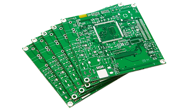
 NextPCB Capabilities
Printed Circuit Boards
NextPCB Capabilities
Printed Circuit Boards
 PCB Assembly
 Layer Buildup
 SMD-Stencils
 PCB Design-Aid & Layout
 Mechanics
 Quality
 Drills & Throughplating
 Factory & Certificate
 PCB Assembly Factory Show
Certificate
PCB Assembly Factory Show
Certificate
Support Team
Feedback:
support@nextpcb.com


Printed Wiring Board (PWB) technology has developed ways to enhance the Interconnection density of the substrate in accordance with the continued rise in component performance and lead density as well as the reduction in package sizes.
Therefore, traditional PWB technology has reached a point where new strategies for providing high-density interconnection (HDI) need to develop. Engineers use HDI technology in all fields owing to its reliability, performance, lightweight properties, and size. And this is essential due to the introduction and ongoing improvement of packaging techniques like
Printed wiring board technology has reached the point where High-density interconnects (HDI), the interconnection revolution, or the density revolution have all been used to describe this phenomenon because it was no longer adequate to carry out the same tasks in a smaller space.
Printed circuit boards with high-density interconnect, or HDI, have more wiring per unit space than conventional printed circuit boards. We consider microvias, blind and buried vias, built-up laminations, and high signal performance like the HDI PCBs.
The development of printed circuit boards has kept pace with the need for smaller and faster products as technology has changed. The vias, pads, copper traces, and gaps on HDI boards are all smaller. Since HDIs have denser wiring, their PCBs are smaller, lighter, and have fewer layers. Manufacturers can replace one HDI board's functionality with several PCBs that we use previously in a device.
We can use different charts and images to explain & comprehend interconnect density though their full extent is not always visible in the below chart 1.1 image. And we are going to use 1.1 and 1.2 to define and comprehend these interconnect density issues and relative factors.
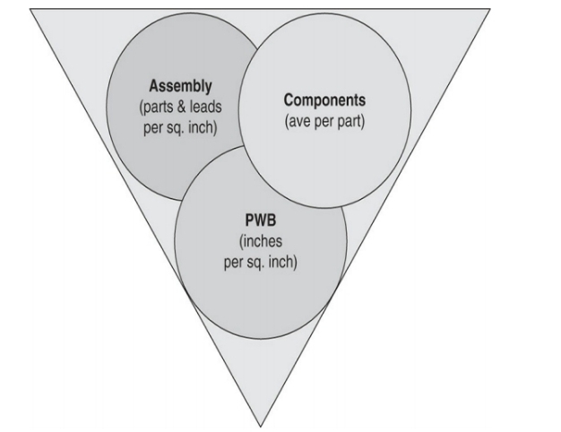
We show the relationship between component packing, surface mount technology (SMT) assembly, and PWB density in the image. It is obvious & clear how these three things are related to one another. The entire connection density is significantly impacted if any changes arise to any one of them. The metric of these three functions is as follows.
We define assembly complexity to measure the difficulty of surface-mounted component assembly in terms of leads and parts per square inch.
Component packaging complexity is defined and serves as a proxy for its level of sophistication to measure the average leads (I/Os) per part of a component.
The quantity of wires in a PWB as measured by the whole area of that board, including all signal layers, or by the average length of traces per square inch. We use Inches per square inch in measurement.
Use of different metrics in different technologies.
Fig. 1.1 depicts the metrics used in assembly, component, and PWB technologies as well as how they generally relate to one another.
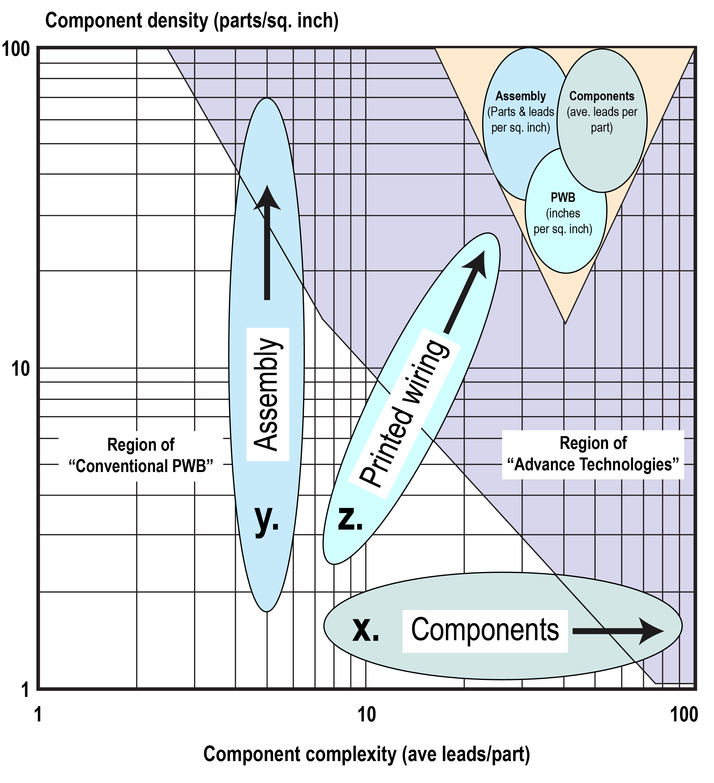
Fig.1.2 This Component technology map illustrates the impact of PWB, assembly, and component technologies on overall package technology and density.
Further, fig.1.2 also explains the interconnection density is the barrier that separates PWB technologies from HDI technologies. Traditional PWB technologies are on the one side most cost-effective when used in this manner. But HDI technologies also exist on the other side of the HDI wall—and they become more cost-effective at some point as well.
In the above-stated Fig. 1.2, we observe how the three elements are related to one another. The picture displays these components as axes of a three-dimensional technology map that depicts the transition from traditional PWB structures to advanced technologies and demonstrates how changes to even a single component can decrease or increase in efficiency and could lessen the electrical package's overall density.
We multiply the total component connections (I/Os), which include both sides of an assembly as well as edge fingers or contacts, by the total number of parts on the assembly to get the part's complexity of the assembly. And manufacturer provides the x-axis as the average leads (I/Os) per part that result.
The x-axis of Fig. 1.1 is made up of the average leads (I/Os) per part which is the result shown in Fig. The horizontal oval shape demonstrates how component complexity can range from discrete circuit elements with two leads per part to BGA and application-specific integrated circuits with extremely huge numbers.
When we discuss the surface-mount assemblies, the vertical (y-axis) dimension (shown by a vertical oval) reflects how difficult it is to build the board in terms of the number of components per square inch or square centimeter of PWB's surface area.
The components per square inch for this vertical oval can range from 1 to over 100. This number automatically increases as the parts get smaller and more compact. Average leads (I/Os) per square inch or square centimeter is a second assembly metric. This results from multiplying the x-axis value by the y-axis value.
We show them he density of the printed wiring board (PWB) in the oval on the z-axis in Fig. 1.2. This is the wiring need, where we assume three nodes per net, to connect all the I/Os of the components at the assembly size provided. An axis can be either centimeters per square centimeter or inches per square inch.
We will examine and demonstrate how the interconnect technology has evolved and is continuing to change, its pace of change, and the direction of these changes by tracking goods of a specific type across time in the below stated Figure. Let's understand this case study in Fig. 1.3.
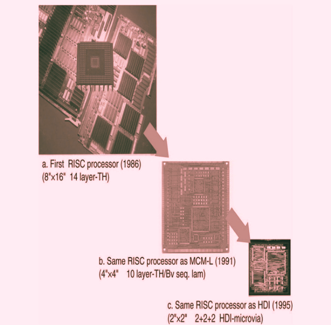
Fig. 1.3 illustrates the same Computer CPU board usage in Components, in Assembly, and in PWB technologies. In the first image (a) we can see the appearance and size of each generation, in (b) we see the movement of board density from traditional to HDI, and in C only HDI. Similarly, different layers of the board were used in all three images. From a 10-layer surface-mount technology board with a surface area of 16 in² 1991 (Fig. 1.3b) to a high-density interconnect board with sequential through-hole 14-layer board with a surface size of 128 in² in 1986 (Fig. 1.3a), the surface area of 4 in² and build-up microvias, buried and blind vias in 1995 (Fig. 1.3c).
To conclude, we thoroughly went through the Interconnection density and how it works with different examples. We also explain high-density interconnection with a map. If you have any questions regarding the HDIs let us know in the comment section. Happy reading!
Still, need help? Contact Us: support@nextpcb.com
Need a PCB or PCBA quote? Quote now


 Surface

