
 NextPCB Capabilities
Printed Circuit Boards
NextPCB Capabilities
Printed Circuit Boards
 PCB Assembly
 Layer Buildup
 SMD-Stencils
 PCB Design-Aid & Layout
 Mechanics
 Quality
 Drills & Throughplating
 Factory & Certificate
 PCB Assembly Factory Show
Certificate
PCB Assembly Factory Show
Certificate
Support Team
Feedback:
support@nextpcb.com


Table Content
Regarding printed circuit boards (PCBs), vias play an important role in connecting different layers and conducting heat. There are two types of vias: blind vias and buried vias. Blind and buried vias are small cylindrical holes that connect different layers of a circuit board. Blind vias connect the outermost layers to one or more internal layers, while buried vias connect two or more internal layers. Blind vias are visible from either the top or bottom side of the circuit board, while buried vias are not visible to the naked eye.
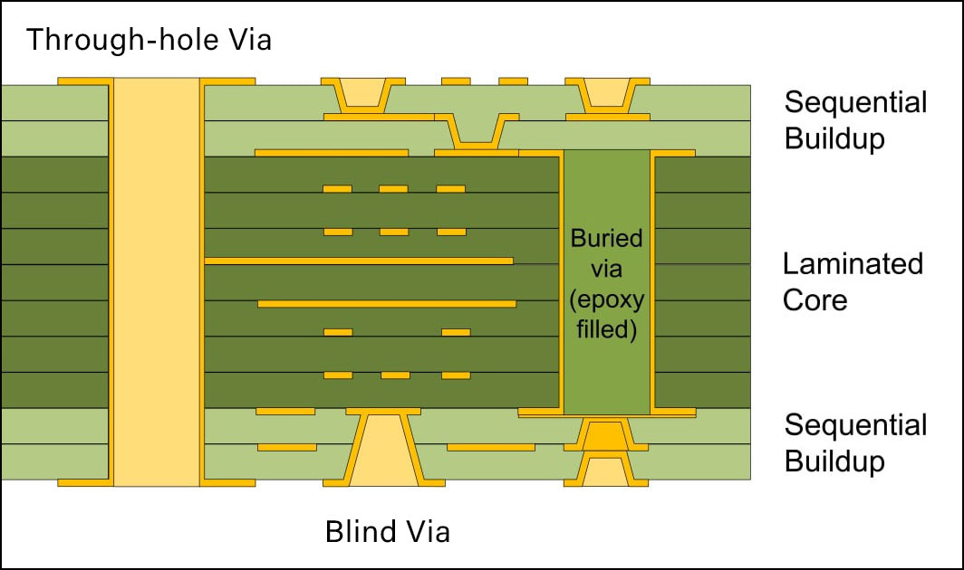
Blind vias are drilled holes that connect the outermost layers of a PCB to one or more internal layers, but they do not go through the entire board. This means that they are only visible from either the top or bottom side of the board, hence the name "blind" vias.
Blind vias are typically used in high-density PCBs where space is at a premium, as they allow designers to pack more circuitry onto the board. They can also be used to route signals from the surface layer to the inner layers, allowing for more efficient signal routing. Additionally, blind vias can be used to reduce the amount of drilling required, which can help to reduce the cost of manufacturing.
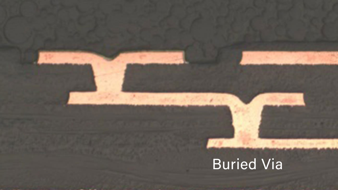
Buried vias are drilled holes that connect two or more internal layers of a PCB, but they do not go through the outer layers of the board. This means that they are not visible from the outside, hence the name "buried" vias.
Buried vias are typically used in multilayer PCBs where several internal layers need to be connected. By using buried vias, designers can reduce the number of through-hole vias that are required, which can improve signal integrity and reduce the risk of interference. Buried vias can also help to reduce the overall size of the PCB, as they allow for more efficient use of space.
The primary difference between the blind and buried via is that the blind vias connect the top layer with the internal layers or with the bottom layer. It is visible from the surface of the printed circuit board. On the other hand, the buried via only connects two or more internal layers. They have no connection with the top or bottom layer of the circuit board. Hence, they are termed buried vias as they do not have anything to do with the outermost layers, which is why they are not visible and can only be traced through the PCB documentation (layout or schematic).
The blind and buried vias have several advantages and serve multiple purposes. The role of vias in a circuit board is undeniable. We need vias either to connect two layers or to faster heat dissipation.
Adjust in Small
Many devices have limited space for the circuit board. In such circumstances, adding the vias in the PCB helps increase the number of layers to reduce the PCB size and route the signal tracks appropriately. Adding blind and buried vias in the space-limited circuit boards helps reduce the circuit complexity and maintain the temperature.
The blind and buried vias are highly applicable in HDI PCBs. We need them in the HDI circuit boards to connect several layers and signal tracks.
Dissipate Heat
The blind and buried vias use to control the heat in the circuit boards. The vias are placed around the heat-generating sources to travel the heat from one conducting layer to another to speed up the heat dissipation. The vias play a vital role in multi-layer boards of up to 20 layers. As in these circuit boards, the circuitry is excessively complex, and heat generation is usually more than the standard PCBs. To manage this heat, the designers place a blind via near the heat-generating components, which increases the rate of heat dissipation and protects the PCB against heat damage.
Escape Routing
Escape routing is a technique of routing connections between components. This routing technique is not a lot different than the standard routing, but the only thing that is a major focus of this technique is minimizing the track span. In escape routing, the designer usually routes the track on a layer, providing a more straight and simple path to connect two components. The vias are used in escape routing to help simplify the circuit and establish a better continuity between the tracks by transferring the signal tracks from one layer to another.
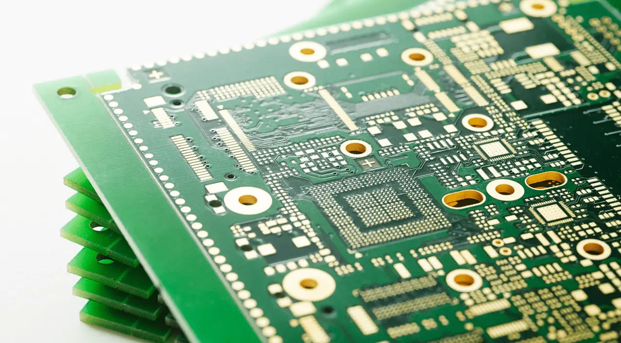
PCB manufacturing itself is a very complex procedure. Converting layouts generated on a computer into a real-time circuit board takes work. PCB manufacturing follows a complicated process to produce well-functioning circuit boards. The PCBs are mainly divided into three categories single, double, and multi-layer circuit boards. The multi-layer PCBs are more complex to manufacture and may involve up to 20 steps. Each step in PCB manufacturing is of great importance and requires skilled hands to perform appropriately.
A multi-layer PCB is a stack of copper-clad laminates separated with prepreg, tightly bound, and cured at a high temperature to melt prepreg to form a strong bond among the laminates. The manufacturing process of a multi-layer PCB starts with the printing of each layer of PCB on a different sheet through a UV printer using photosensitive ink. These printed layers are also called blueprints. Then the copper-clad laminates, which are nothing special than a thick sheet of dielectric material (i.e., FR-4) coated with copper from both sides, are pressure washed and cleaned. After this, the blueprints are converted onto the cleaned laminates and cured under UV light to harden the PCB tracks. Then these laminates are pressure washed with an alkaline solution to dissolve the excess copper from the laminates. Once all the inner and outer layers are printed and etched, these boards are properly aligned and screwed between two heavy metallic plates to build pressure on the individual layers. Then this stack is put under the curing ovens at a high temperature to melt the prepreg between the laminates. The prepreg serves as an adhesive material for laminates to bond them together.
Related: A Step-by-Step Guide to PCB Manufacturing Process
Once all the internal layers have been printed and stacked by the manufacturer, the top and bottom layers are printed and etched, and then the stack finally goes for the drilling and then for surface finish and silk screening.
During this PCB manufacturing process, the vias get drilled according to their nature and specification. The manufacturer drills blind vias while drilling holes when the stack is complete. However, the buried vias are prepared before stacking and laminating different cores. It is because once all the individual laminates are stacked together, it will be impossible to drill a hole in the internal layers without leaving traces on either the top or the bottom layer.
The manufacturing of blind and buried vias consists of several more steps compared to the manufacturing of a standard via. When it comes to blind vias, a hole is drilled through the board from the top or bottom side, and then the hole is filled with a conductive material through electroless or electroplating. For buried vias, a small hole is drilled from one inner layer to another and then filled with a conductive material using the same procedure, electroless or electroplating. The challenge faced in manufacturing both vias is ensuring that the hole is properly aligned with the intended layers and that the conductive material covers the entire hole without leaving any voids.
The selection of Blind vs. Buried Via depends on multiple factors. It includes whether you have to make a connection between surface mount devices and the internal layers of the circuit board or you have to connect two internal layers and fasten up the heat dissipation.
However, following the general practices, if you have a high-density circuit design with limited space, blind vias can be a better choice. On the other side, if the circuit board consists of several layers stacked together and has limited space but requires a lot of connections in the internal layers, buried vias may be a better choice.
A PCB via is a small hole like one for the through-hole component. The function of a via is to connect two or more than two internal or external layers together or with each other. On a broad level, we divide PCB vias into three categories blind vias, buried vias, and through-hole vias.
A buried via exists in the internal layers of the circuit board and can not be seen by the naked eye. It uses to connect two or more internal layers or signal traces present on different layers of the circuit board. On the other side, a blind via connects the top or bottom layer with one or more than one internal layer(s). Hence blind vias can be seen from the naked eye from one side of the board. It is because they pass a partial width of the board. Blind vias have a quite similar function as buried vias.
Both blind and buried vias have their own advantages and disadvantages that we have explained in detail in this article. However, the selection of the appropriate type of via depends on the design and requirements of the circuit board.
Still, need help? Contact Us: support@nextpcb.com
Need a PCB or PCBA quote? Quote now


 Surface

