
 NextPCB Capabilities
Printed Circuit Boards
NextPCB Capabilities
Printed Circuit Boards
 PCB Assembly
 Layer Buildup
 SMD-Stencils
 PCB Design-Aid & Layout
 Mechanics
 Quality
 Drills & Throughplating
 Factory & Certificate
 PCB Assembly Factory Show
Certificate
PCB Assembly Factory Show
Certificate
Support Team
Feedback:
support@nextpcb.com


Nearly every digital circuit is made up of IC (incorporated circuit) as well as ICs have actually come to be an essential element in sophisticated electronic devices. The style and also growth of ICs have actually carefully progressed for many years; ICs have actually ended up being portable, much less power consuming, as well as extra useful. However, this modification included advancement in IC product packaging; the IC product packaging has actually developed with time. Today, developers can select between product packaging kinds according to job expediency.
The development in IC product packaging began in the 1970s as well as ever since, the IC plans have actually developed to a level that today, a Micro SD flash memory card holds a lot more information than a substantial disk drive carried out in the 20th century.
Integrated circuits are created with semi-conductors that are tiny as well as fragile. Provided the little dimension of semi-conductors, a physical link in between the semiconductor chips and also the circuit is difficult and also not practical. In addition, the chips need to be secured versus rust and also any type of undesirable electric get in touch with.
The elements are selected, put, and also set up on the PCB making use of unique tools. The manufacturing procedure is much less taxing yet provided the tiny dimension of SMDs, manufacture can be difficult. When several SMDs are positioned better, troubles can develop as well as their discovery is additionally hard.
The variety of pins is generally in several of 4, the real estate is normally rectangle-shaped. Nonetheless, the form can be various for some gadgets; relying on the interior design.
Mainly, there are just 2 kinds of IC bundles: Through-hole and also SMD (surface area place gadget) yet there are numerous sub-types.
Requirement through-hole plan is one of the most generally utilized kinds of the through-hole bundle in commercial production. The conventional through-hole bundle preserves a 0.1" range in between surrounding pins however there is no certain order of pins like in DIP.
The pins prolonged from the within to the best angle in the direction of an all-time low. The range in between all nearby pins is 0.1".
Yet exactly how do IC product packaging kinds influence the effectiveness of digital motherboards? The response stays with the features of IC product packaging.
The elements are selected, put, and also set up on the PCB making use of unique tools. The manufacturing procedure is much less taxing yet provided the tiny dimension of SMDs, manufacture can be difficult. When several SMDs are positioned better, troubles can develop as well as their discovery is additionally hard.
A few of the typical kinds of through-hole bundles are as adheres to.
Typically, through-hole gadgets are typically utilized. They have actually legs prolonged sufficient to experience openings in PCB (published circuit card). The tools are put on one side of the PCB and also soldered beyond.
ZIP parts likewise have pins expanded outside, in the direction of all-time low yet they are a little bit transformed near the top. ZIP parts did not obtain appeal as a result of their curved style which triggered difficulties throughout putting together procedure.
SMDs are portable as well as costly as contrasted to through-hole product packaging. Yet their portable dimension additionally allows the advancement of massive circuits on the fine print circuit board. Furthermore, they do not call for hole-drilling for pin soldering; all pins as well as the product packaging lie on the very same side of the board.
Reduce bundle parts are additionally the like conventional through-hole parts other than, reduce elements are smaller sized as well as they have a 0.07" range in between pins. Reduce product packaging is normally utilized for parts that have numerous pins as well as need to be established in a smaller sized dimension.
Nonetheless, in the very early years of its advancement, ZIP parts were favored in DRAM (vibrant arbitrary accessibility memory) advancement. Yet today, ZIP parts are hardly ever or no more established because of no need.
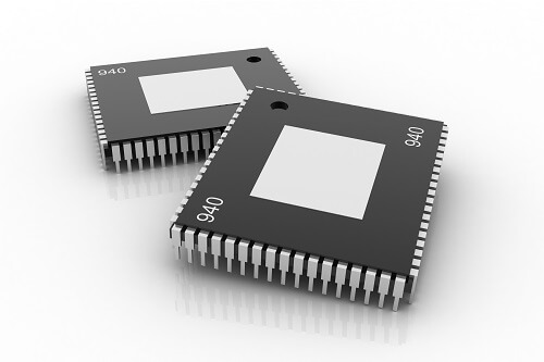
Surface Area Mount Modern technology is the 2nd most frequently made use of innovation of IC product packaging for commercial-scale production. The elements created with SMT are called SMD (surface area install gadgets).
To safeguard chips as well as establish IC pins to ensure that the semiconductor can be gotten in touch with the circuit, they are housed inside a bundle. The plan can be smaller sized than your nails or it can be bigger; depending upon the bundle kind.
Given that through-hole elements are basic, they are much less expensive as contrasted to surface area install gadgets. This is why a lot of inexpensive electronic devices make use of through-hole elements. Nonetheless, through-hole parts are numerous times larger than surface-mount tools which imply they call for even more room aboard.
DIP has additional sub-types yet one of the most typical kinds are MDIP (shaped double in-line plan) and also PDIP (plastic double in-line plan).
2 simplicity SMD putting together and also mistake discovery, L-shaped Lead Plan as well as Sphere Grid Selection are utilized. Both kinds are frequently made use of on a commercial range.
Like in various other sorts of plans, the BGA real estate additionally a little differs from IC to IC however generally plastic real estate is utilized for confining the SMD chip.
BGA product packaging lugs an SMD chip however in a different way; the pins are not the only component that can be found in contact with all-time low, rather the entire base of BGA remains on the board. The all-time low is made up of tiny leads that develop contact with the circuit.
BGA product packaging is generally utilized in high-speed applications particularly computer systems. They can be seen on motherboards in computer systems.
As the name recommends, the leads/pins of these SMDs are L-shaped. They expand out of the element real estate, go up and down downward, and afterward take an appropriate angle; obtaining alongside the board that makes an L-shape. This L-shape maintains the leads in straight instructions to the boards which relieve the setting up procedure.
L-shaped Lead Bundles are generally utilized in arbitrary accessibility memory and also power blink memory advancement.
Still, need help? Contact Us: support@nextpcb.com
Need a PCB or PCBA quote? Quote now


 Surface

