Table of Contents
- I. Overview of Specifications
- II. Static Characteristics: The Deeper Relationship Between Temperature and Efficiency
- 1. The Risk of Thermal Runaway in RDS(on)
- 2. Leakage Current (IDSS) and High-Temperature Standby
- 3. Threshold Voltage (VGS(off)) Drift
- III. Dynamic Characteristics and Switching Loss Calculation
- 1. Parasitic Capacitance vs. Temperature
- 2. Switching Loss Calculation (Psw)
- IV. Thermal Design and Package Selection
- 1. Impact of Package on Heat Dissipation
- 2. Thermal Management Strategy
- V. Advanced Design: EMI, Reliability, and Driver Optimization
- 1. EMI and Noise Control
- 2. Optimizing the Gate Drive Circuit
- 3. Body Diode and Reliability
- Summary
In power supply design, motor drives, and various switching circuits, the Power MOSFET is the core execution component. However, when selecting a component, many engineers often focus solely on Breakdown Voltage (VDSS) and Current (ID), ignoring other critical electrical characteristics hidden deep within the datasheet.
Based on the measured data of a typical 60V high-current Power MOSFET, this article will fully display its specifications and deeply analyze its static characteristics, dynamic switching characteristics, thermal management, and reliability design. We will take you behind the scenes of the attractive 4.3mΩ low on-resistance figure to reveal the hidden driving challenges and design trade-offs involved.
> Learn How Does a MOSFET Work?
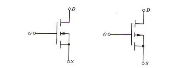
Device symbol
Picture resource: Kaur, R., Gupta, P., & Singh, J. (2017). A review on power MOSFET device structures. International Journal for Research in Applied Science & Engineering Technology (IJRASET), 5(X). Retrieved from https://www.researchgate.net/publication/350889967_A_Review_on_Power_MOSFET_Device_Structures
I. Overview of Specifications
Below is the complete electrical characteristics table for this Power MOSFET. We will use this table as a blueprint for our subsequent analysis.
| Item |
Symbol |
Min |
Typ |
Max |
Unit |
Test Conditions |
Temp. Dependency |
Design Considerations |
| Drain-Source Breakdown Voltage |
VBRSS |
60 |
- |
- |
V |
ID = 10mA, VGS = 0 |
↑ |
Related to On-Resistance. |
| Drain Cut-off Current |
IDSS |
- |
- |
10 |
μA |
VDS = 60V, VGS = 0 |
↑ |
Affects noise in switching travel and switching times tr, tf. |
| Gate Cut-off Current |
IGSS |
- |
- |
±0.1 |
μA |
VGS = ±20V, VDS = 0 |
- |
- |
| Gate-Source Cut-off Voltage |
VGS(off) |
1.0 |
- |
2.5 |
V |
VDS = 10V, ID = 1mA |
↓ |
Products with internal holding diodes range from hundreds of nA to μA; spec value is ±10μA. |
| Forward Transfer Admittance |
|Yfs| |
55 |
90 |
- |
S |
ID = 45A, VDS = 10V |
↓ |
Affects noise in switching travel and switching times tr, tf. |
| Static Drain-Source On-Resistance 1 |
RDS(on)1 |
- |
4.3 |
5.5 |
mΩ |
ID = 45A, VGS = 10V |
↑ |
The most important parameter determining conduction loss. Note that it increases as temperature rises. |
| Static Drain-Source On-Resistance 2 |
RDS(on)2 |
- |
6.0 |
9.0 |
mΩ |
ID = 45A, VGS = 4V |
↑ |
The most important parameter determining conduction loss. Note that it increases as temperature rises. |
| Input Capacitance |
Ciss |
- |
9770 |
- |
pF |
VDS = 10V, VGS = 0, f=1MHz |
- |
Dependent on VDS: Indicator of drive loss during analog operation. |
| Output Capacitance |
Coss |
- |
1340 |
- |
pF |
VDS = 10V, VGS = 0, f=1MHz |
- |
Dependent on VDS: Affects fall time tf under light loads. |
| Reverse Transfer Capacitance |
Crss |
- |
470 |
- |
pF |
VDS = 10V, VGS = 0, f=1MHz |
- |
Dependent on VDS: Affects switching times tr, tf. |
| Total Gate Charge |
Qg |
- |
180 |
- |
nC |
VDD = 50V, VGS = 10V, ID = 85A |
- |
Determines pull-in specifications; highly dependent on gate drive voltage. |
| Gate-Source Charge |
Qgs |
- |
32 |
- |
nC |
VDD = 50V, VGS = 10V, ID = 85A |
- |
- |
| Gate-Drain Charge |
Qgd |
- |
36 |
- |
nC |
VDD = 50V, VGS = 10V, ID = 85A |
- |
Characteristic determining switching times tr, tf: Dependent on supply voltage VDD (increases as VDD rises). |
| Turn-on Delay Time |
td(on) |
- |
53 |
- |
ns |
VGS = 10V, ID = 45A, RL = 0.67Ω, Rg = 50Ω |
- |
Depends on Rg, Qgd, and gate drive voltage. |
| Rise Time |
tr |
- |
320 |
- |
ns |
VGS = 10V, ID = 45A, RL = 0.67Ω, Rg = 50Ω |
- |
Depends on Rg, Qgd, and gate drive voltage; affects maximum jump amplitude of frequency variation. |
| Turn-off Delay Time |
td(off) |
- |
700 |
- |
ns |
VGS = 10V, ID = 45A, RL = 0.67Ω, Rg = 50Ω |
- |
Affects switching speed. |
| Fall Time |
tf |
- |
380 |
- |
ns |
VGS = 10V, ID = 45A, RL = 0.67Ω, Rg = 50Ω |
- |
Affects switching speed. |
| Diode Forward Voltage |
VDF |
- |
1.0 |
- |
V |
IF = 85A, VGS = 0 |
↓ |
Becomes an On-Resistance related characteristic if bias is applied to VGS. |
| Diode Reverse Recovery Time |
trr |
- |
70 |
- |
ns |
IF = 85A, VGS = 0, di/dt = 50μA/μs |
↑ |
Reduce di/dt to control short-circuit current and noise. |
Note: ↑: Positive temperature coefficient; ↓: Negative temperature coefficient.
II. Static Characteristics: The Deeper Relationship Between Temperature and Efficiency
Static characteristics describe the MOSFET's performance in a steady state. Beyond basic voltage ratings and resistance, the impact of temperature is an "invisible killer" that must be considered in design.
1. The Risk of Thermal Runaway in RDS(on)
The table shows that at VGS = 10V, the typical RDS(on) is 4.3 mΩ.
- Temperature Dependency: RDS(on) has a significant positive temperature coefficient (↑). At a junction temperature of 175°C, the resistance value is typically 1.5 to 2 times that at room temperature.
- Design Insight: If you calculate full-load power loss using the room temperature value of 4.3 mΩ, the resistance will increase as the device heats up during actual operation. This generates more heat, further increasing resistance, and potentially leading to Thermal Runaway. It is recommended to perform thermal evaluation using at least 1.5 × RDS(on).
2. Leakage Current (IDSS) and High-Temperature Standby
The maximum leakage current is 10μA. While this seems negligible at room temperature, it rises exponentially with temperature. In high-temperature environments (e.g., above 100°C), leakage current can increase to the mA level. For low-power or battery-operated devices, this is a significant source of standby power loss that cannot be ignored.
3. Threshold Voltage (VGS(off)) Drift
VGS(off) has a negative temperature coefficient (↓). As temperature rises, the MOSFET becomes easier to turn on. In high-temperature environments with noise interference, if there is insufficient gate turn-off negative voltage or pull-down resistance, false triggering (mis-conduction) may occur, leading to device failure.
III. Dynamic Characteristics and Switching Loss Calculation
For switching power supplies, dynamic parameters directly determine efficiency. Low RDS(on) usually implies a larger die area, which inevitably brings massive parasitic parameters.
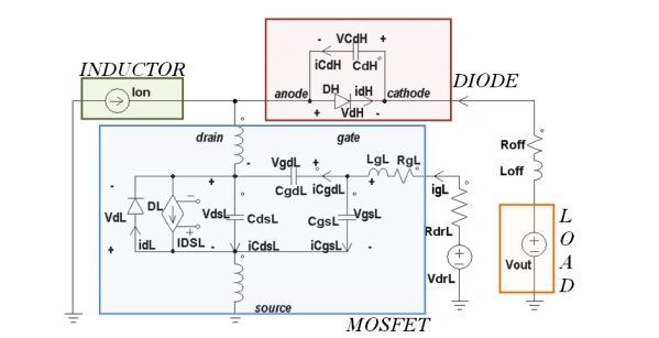
Boost converter case study
Picture resource: Di Capua, G., & co-authors. (2014). Analysis and characterization of power MOSFETs for power converters: Energy & reliability-aware design. Proceedings of the 2014 IEEE International Symposium on Industrial Electronics (ISIE). Retrieved from https://www.researchgate.net/publication/262979854_Analysis_and_Characterization_of_Power_MOSFETs_for_Power_Converters_EnergyReliability-Aware-Design
1. Parasitic Capacitance vs. Temperature
- Ciss (9770 pF): Although capacitance itself is not sensitive to temperature, this massive value is a severe test for the driver circuit.
- Crss (470 pF): This determines the duration of the Miller Plateau. Note that these capacitance values change drastically with VDS voltage. At low voltages, Ciss and Crss increase significantly, making driving during the soft-start phase much more difficult.
2. Switching Loss Calculation (Psw)
The switching times given in the table (tr=320ns, tf=380ns) were measured under Rg=50Ω. In practical applications, switching loss Psw can be estimated using the following formula:
Psw ≈ 1/2 × VDS × ID × (tr + tf) × fsw
- Case Analysis: Assuming VDS=48V, ID=20A, fsw=100kHz, if we do not optimize the driver and directly use the table values for tr, tf (total 700ns):
- Psw ≈ 0.5 × 48 × 20 × 700 × 10-9 × 100 × 103 ≈ 33.6W
Conclusion: A switching loss of 33.6W is unacceptable! This indicates that you must significantly reduce Rg and use a powerful gate driver to compress tr/tf to the tens of nanoseconds range to use this device at high frequencies.
IV. Thermal Design and Package Selection
For high-power devices, it is not enough to just "calculate" the heat; you must also "dissipate" it.
1. Impact of Package on Heat Dissipation
With currents reaching dozens of Amperes, the Thermal Resistance (Rθ) of the package is critical.
- TO-220 (Through-Hole): Suitable for applications requiring large external heatsinks. Its Junction-to-Case thermal resistance (RθJC) is typically low, offering high heat dissipation potential.
- D2PAK (Surface Mount): Suitable for automated manufacturing. Heat dissipation relies mainly on the copper foil area or aluminum substrate on the PCB. At high currents, sufficient copper pouring area and Thermal Vias must be designed to reduce Junction-to-Ambient thermal resistance (RθJA).
2. Thermal Management Strategy
- Calculate Junction Temperature: Tj = Ptotal × RθJA + Ta. Ensure Tj remains below 150°C or 175°C under worst-case conditions.
- Active Cooling: When natural convection is insufficient, consider forced air cooling or liquid cooling. For this MOSFET, since RDS(on) is extremely low, conduction loss is relatively small, but in high-frequency applications, massive switching losses may become the main heat source.
V. Advanced Design: EMI, Reliability, and Driver Optimization
1. EMI and Noise Control
To reduce losses, we tend to increase switching speed (reduce Rg), but this increases di/dt and dv/dt, leading to severe Electromagnetic Interference (EMI).
- Balancing Act: Placing an appropriate resistor Rg in series with the gate is key to balancing efficiency and EMI.
- Layout Optimization: Minimizing the area of the Power Loop and the Gate Loop is the most effective way to reduce radiated noise.
- Snubber Circuit: Paralleling an RC snubber circuit between the drain and source can effectively suppress high-frequency oscillation spikes caused by parasitic inductance, protecting the device and improving EMI.
2. Optimizing the Gate Drive Circuit
Facing a massive Qg of 180 nC and Ciss of 9770 pF, a standard MCU IO pin (typically only 20mA drive capability) is completely inadequate.
- Drive Current Calculation: To complete switching within tsw = 100ns, the required drive current is Ig ≈ Qg / tsw = 180nC / 100ns = 1.8A.
- Selection Advice: You must select a dedicated Gate Driver chip with a peak current capability of 2A ~ 4A.
3. Body Diode and Reliability
- Reverse Recovery (trr=70ns): In synchronous rectification or bridge circuits, the reverse recovery of the body diode generates additional loss and noise. While 70ns is a decent spec, in high-frequency applications, be wary of the Irr current spikes it brings.
- ESD and SOA: In inductive load applications like motor drives, ensure the MOSFET operates within the Safe Operating Area (SOA). For the gate, it is recommended to add Zener diodes for ESD protection to prevent static electricity or overvoltage from punching through the fragile gate oxide layer.
Recommend reading:
> PMOS VS NMOS: Focus on Two Main Forms of MOSFET
Summary
This 60V MOSFET is a device with typical "distinct pros and cons":
- Pros: Extremely low on-resistance (4.3mΩ), making it the king for high-current, low-frequency (<50kHz) load switching or motor drive applications.
- Challenge: Massive input capacitance and gate charge make it unsuitable for direct use in high-frequency switching power supplies (e.g., >200kHz) unless paired with an extremely powerful drive circuit and accepting certain switching losses.
Final Design Recommendation
In summary, the choice of Power MOSFET should depend on the specific application:
- 1. Low-Frequency, High-Current Applications (e.g., motor drives): This MOSFET's low on-resistance (4.3mΩ) is ideal for high-current, low-frequency applications. However, ensure you use a strong gate driver due to the high input capacitance.
- High-Frequency Switching (e.g., switching power supplies): Due to its large gate charge and parasitic capacitance, this MOSFET is not suitable for high-frequency applications (>200kHz) without a high-performance gate driver.
- Thermally Constrained Environments: While it offers low conduction loss, its on-resistance increases with temperature. Proper heat dissipation is essential to prevent thermal runaway.
- Battery-Powered Applications: This MOSFET may not be ideal due to its leakage current and high gate charge. For such applications, choose MOSFETs with lower leakage and gate charge.
Choose the MOSFET based on your application's current, frequency, and thermal needs while ensuring proper gate drive and heat management. For high-quality PCB manufacturing and assembly solutions, NextPCB offers advanced services to meet your design and production needs.
Visit NextPCB to explore our capabilities and get started with your custom PCB orders today!
You may also interested in:
> IRFZ44N: The Ultimate Guide to This Powerful MOSFET Transistor
> How to Test MOSFETs: A Comprehensive Guide
About the Author
Arya Li, Project Manager at NextPCB.com
With extensive experience in manufacturing and international client management, Arya has guided factory visits for over 200 overseas clients, providing bilingual (English & Chinese) presentations on production processes, quality control systems, and advanced manufacturing capabilities. Her deep understanding of both the factory side and client requirements allows her to deliver professional, reliable PCB solutions efficiently. Detail-oriented and service-driven, Arya is committed to being a trusted partner for clients and showcasing the strength and expertise of the factory in the global PCB and PCBA market.

 NextPCB Capabilities
 PCB Assembly
 Layer Buildup
 SMD-Stencils
 PCB Design-Aid & Layout
 Mechanics
 Surface
 Quality
 Drills & Throughplating
 Factory & Certificate


