NextPCB Capabilities
Printed Circuit Boards
NextPCB Capabilities
Printed Circuit Boards
 PCB Assembly
 Layer Buildup
 SMD-Stencils
 PCB Design-Aid & Layout
 Mechanics
 Quality
 Drills & Throughplating
 Factory & Certificate
 PCB Assembly Factory Show
Certificate
PCB Assembly Factory Show
Certificate
Support Team
Feedback:
support@nextpcb.com


Introduction
The world of electronic components is huge and dynamic, with MOSFETs (Metal-Oxide-Semiconductor Field-Effect Transistors) holding a crucial position. When it comes to MOSFETs (Metal-Oxide-Semiconductor Field-Effect Transistors), there are two main types that dominate the field: PMOS (P-channel MOSFET) and NMOS (N-channel MOSFET). These complementary types of MOSFETs play a crucial role in modern electronics, and understanding PMOS VS NMOS: Focus on Two Main Forms of MOSFET and how mosfets work, What is Pmos?, What is Nmos?, p mosfet vs n mosfet is essential for anyone interested in the field.
PMOS is a type of MOSFET where the majority charge carriers are holes. It is designed to operate with a positive voltage supply. In a PMOS transistor, the source and drain regions are doped with n-type material, while the channel is doped with p-type material. When a positive voltage is applied to the gate terminal, it creates an electric field that attracts the holes, allowing current to flow from the source to the drain. On the other hand, NMOS is a type of MOSFET where the majority charge carriers are electrons. It operates with a negative voltage supply. In an NMOS transistor, the source and drain regions are doped with p-type material, while the channel is doped with n-type material. When a negative voltage is applied to the gate terminal, it creates an electric field that attracts the electrons, allowing current to flow from the source to the drain.
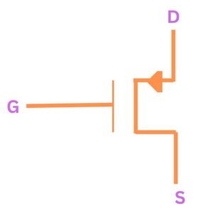
What is PMOS? - PMOS, short for P-channel Metal-Oxide-Semiconductor, is a type of field-effect transistor (FET) commonly used in electronic devices and integrated circuits. It is the counterpart to NMOS (N-channel Metal-Oxide-Semiconductor) and together they form the foundation of modern digital electronics. PMOS transistors are designed to operate with a positive voltage applied to the gate terminal, which creates a conducting channel between the source and drain terminals. This means that when the gate voltage is low, the transistor is "on" and allows current to flow. Conversely, when the gate voltage is high, the transistor is "off" and restricts the flow of current.
PMOS technology uses low power consumption. Since PMOS transistors operate with a positive gate voltage, they are ideal for applications where the majority of the time is spent in an "off" state. This makes them particularly suitable for use in static memory cells and other low-power circuitry. PMOS technology has been widely used in various electronic devices, including smartphones, tablets, and computers. Its reliability and efficiency have made it a popular choice among manufacturers and engineers.
PMOS Transistor
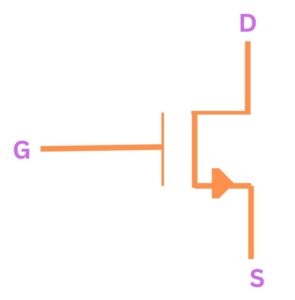
What is Nmos? - NMOS, stands for N-type Metal-Oxide-Semiconductor, is a type of transistor technology commonly used in digital and analog circuits. It is one of the two fundamental types of MOSFET (Metal-Oxide-Semiconductor Field-Effect Transistor) technology, with the other being PMOS (P-type Metal-Oxide-Semiconductor).So, how does NMOS work? In simple terms, it utilizes the movement of electrons to control the flow of current. The transistor consists of a source, a drain, and a gate. When a voltage is applied to the gate, it creates an electric field that allows the flow of electrons from the source to the drain. This flow of electrons forms the basis for the operation of NMOS transistors.
NMOS technology is widely used in various applications, including microprocessors, memory chips, and integrated circuits. It offers several advantages, such as high speed, low power consumption, and compatibility with complementary MOS (CMOS) technology. It's important to note that NMOS symbol technology has been largely replaced by CMOS technology in modern electronic devices. CMOS offers improved power efficiency and reduced power consumption compared to NMOS. However, NMOS still finds its use in specific applications where high-speed operation is crucial.
NMOS Transistors
Order Reliable Components Online
The comparison between PMOS (Positive Metal-Oxide-Semiconductor) and NMOS (Negative Metal-Oxide-Semiconductor) or pmos vs nmos transistors is a pivotal exploration for engineers and electronics enthusiasts. These two fundamental variants of MOSFETs, pmos vs nmos, play integral roles in electronic circuitry, each characterized by distinct charge carriers and semiconductor materials. PMOS transistors employ positive charge carriers or "holes" in a P-type semiconductor, while NMOS transistors symbol utilize negative charge carriers or electrons in an N-type semiconductor. PMOS is known for its slower speed but lower power consumption, making it suitable for low-power applications. NMOS, on the other hand, offers faster speed but higher power consumption, making it ideal for high-performance applications. Here are detailed overview of comparing PMOS and NMOS :
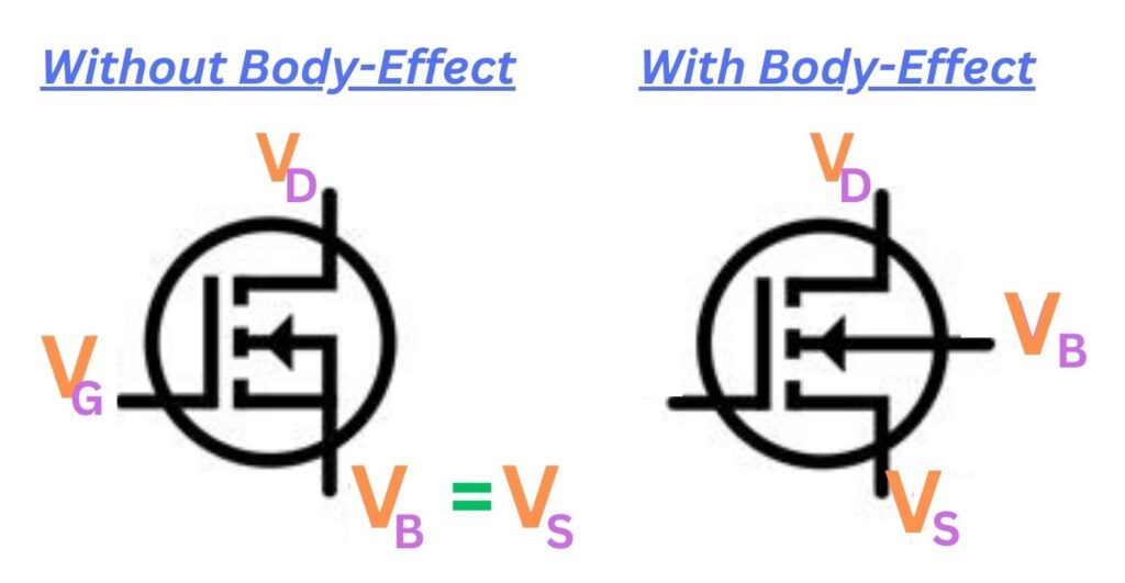
The Metal-Oxide-Semiconductor Field-Effect Transistor (MOSFET) is a crucial component in modern electronic devices. It is widely used in applications ranging from power amplifiers to microprocessors. The MOSFET Third Terminal: The Body effect occurs due to the interaction between the body terminal and the channel region of the MOSFET. The channel region is formed between the source and drain terminals, and it controls the flow of current in the device. By applying a voltage to the body terminal, the characteristics of the channel region can be modified. One of the main body effect of mosfet third terminal bias is the control of the threshold voltage. The threshold voltage is the voltage required to turn on the Nmos MOSFET, allowing current to flow through the channel. By adjusting the body bias, the threshold voltage can be increased or decreased, thus controlling the behavior of the MOSFET.
The Body Effect of PMOS and NMOS
While transistor operation is commonly explained by the gate, drain, and source, it's crucial to note that a MOSFET is a 4-pin device. The additional pin is termed the "body" and is linked to the transistor's substrate. If the voltage between the body and source deviates from zero, the transistor experiences the body-effect. This effect alters the threshold voltage (VT) and can be harnessed to dynamically modify transistor properties. Typically viewed as an undesired occurrence, the body-effect arises when the body node isn't directly connected to the source voltage.
In electronic components, the construction and physical operation of PMOS (Positive Metal-Oxide-Semiconductor) and NMOS (Negative Metal-Oxide-Semiconductor) transistors are foundational aspects that underpin their functionality. Construction of PMOS and NMOS Transistor : The construction of a PMOS transistor involves creating a P-type well or substrate within the semiconductor material, with a thin layer of silicon dioxide acting as the insulating oxide layer. The gate terminal is typically made of metal, forming a Schottky barrier with the semiconductor material. This construction facilitates the control of current flow between the source and drain terminals through the application of a positive voltage to the gate. Conversely, NMOS transistors have an N-type well or substrate, and the gate terminal is constructed similarly with a metal layer on top of a silicon dioxide insulator. Applying a negative voltage to the gate in an NMOS transistor symbol controls the flow of electrons between the source and drain terminals, allowing or impeding current conduction.
Physical Operation of PMOS and NMOS transistors : The physical operation of PMOS and NMOS transistors revolves around the modulation of the conductive channel between the source and drain terminals by the voltage applied to the gate. In PMOS transistors, a positive voltage on the gate repels the positively charged holes in the channel, creating a depletion region and reducing the flow of current between the source and drain. Conversely, in NMOS switch transistors, a negative voltage on the gate attracts electrons to the channel, enhancing current flow between the source and drain.
In modern electronics, two key components of circuit designing are NMOS (N-type Metal-Oxide-Semiconductor) and PMOS (P-type Metal-Oxide-Semiconductor) transistors. These transistors are widely used in various applications, from microprocessors to memory chips, and understanding NMOS and PMOS: Utilization is essential for engineers and enthusiasts alike. Both NMOS and PMOS transistors are types of field-effect transistors (FETs) that operate based on the principle of controlling the flow of current using an electric field. The key difference between nmos vs pmos symbol lies in the type of charge carriers they utilize. NMOS transistors use electrons as carriers, while PMOS transistors use holes.
NMOS transistors are commonly used in integrated circuits due to their high switching speed and low power consumption. They are known for their efficiency in digital logic circuits, making them ideal for applications such as microprocessors and memory chips. On the other hand, PMOS transistors are mainly used in low-power applications and analog circuits, where their higher threshold voltage and slower switching speed are less of a concern. Important aspect of NMOS and PMOS : utilization is designing complementary metal-oxide-semiconductor (CMOS) circuits. CMOS circuits combine both NMOS and PMOS transistors to take advantage of their complementary characteristics. By using NMOS switch transistors for the low state and PMOS transistors for the high state, CMOS circuits can achieve low power consumption and high noise immunity.
The switching mechanism of both PMOS and NMOS transistors is rooted in the modulation of their conductive channels. These transistors operate as voltage-controlled switches, where the application of a specific voltage to the gate terminal enables or disables the flow of current between the source and drain terminals. In the case of PMOS switch transistors, a positive voltage applied to the gate creates a repulsive force on the positively charged "holes" within the P-type semiconductor material, depleting the channel and inhibiting current flow. Conversely, NMOS switch transistors operate with a negative gate voltage, attracting electrons to the N-type semiconductor channel, facilitating the flow of current between the source and drain. There exist various configurations for nmos MOSFET switches, as illustrated in the diagram. These include a basic NMOS switch, a bidirectional current-capable transmission gate, and a CMOS digital inverter, which can be viewed as a complementary switch.
NMOS Switch Transmission Gate CMOS Switch
PMOS as a Switch:
NMOS as a Switch:
The utilization of transistors, particularly PMOS (Positive Metal-Oxide-Semiconductor) and NMOS (Negative Metal-Oxide-Semiconductor) transistors, forms the backbone of amplifier design. The amplification dynamics of these transistors, unraveling their distinctive contributions to electronic systems. An amplifier magnifies the strength of a signal, be it voltage, current, or power. PMOS and NMOS transistors, when incorporated into amplifier circuits, modulate the input signal to achieve the desired amplification effect.
PMOS Transistors in Amplifiers : PMOS transistors, operating with positive charge carriers or "holes," contribute to amplification in P-type regions of a semiconductor. In amplifier circuits, a positive voltage applied to the gate terminal controls the flow of holes between the source and drain, effectively amplifying the input signal.
NMOS Transistors in Amplifiers : NMOS transistors, employing negative charge carriers or electrons, are instrumental in amplification within N-type regions of a semiconductor. A negative voltage applied to the gate facilitates the controlled flow of electrons between the source and drain, achieving signal amplification.
In conclusion, comparing PMOS and NMOS, p mosfet vs n mosfet goes beyond just positive and negative charges. It involves understanding PMOS VS NMOS: Focus on Two Main Forms of MOSFET and how they work as switches and amplifiers, impacting the efficiency, speed, and power use of electronic circuits in our connected world. As we wrap up this exploration, the ongoing story of nmos vs pmos transistors, mosfet meaning, how mosfets work shows the constant innovation in electronic engineering. Engineers and enthusiasts can use their knowledge to create advanced technologies, pushing us toward a future where electronic possibilities are limitless.
- IRFZ44N: The Ultimate Guide to This Powerful MOSFET Transistor
- What's the difference between MOSFET and BJT and how to choose?
- Free Worldwide Shipping on Over 600,000 Electronics Components with HQ Online
- Free PCB Assembly Offer is Now Live: Experience Reliable PCB Assembly from HQ NextPCB
- HQ NextPCB Introduces New PCB Gerber Viewer: HQDFM Online Lite Edition
Still, need help? Contact Us: support@nextpcb.com
Need a PCB or PCBA quote? Quote now


 Surface