
 Surface


Julia Wu - Senior Sales Engineer at NextPCB.com

 NextPCB Capabilities
Printed Circuit Boards
NextPCB Capabilities
Printed Circuit Boards
 PCB Assembly
 Layer Buildup
 SMD-Stencils
 PCB Design-Aid & Layout
 Mechanics
 Quality
 Drills & Throughplating
 Factory & Certificate
 PCB Assembly Factory Show
Certificate
PCB Assembly Factory Show
Certificate
Support Team
Feedback:
support@nextpcb.com


Key Takeaways
Whether you're a hardware engineer, startup founder, or high-volume manufacturer, understanding how SPI prevents defects, reduces rework costs, and enhances long-term reliability is essential for successful PCB assembly.
In the field of electronics manufacturing, prototype failure often results in high costs in terms of both time and money. While engineers sometimes blame soldering issues on chip failures or improper reflow temperature profiles, industry data reveals a critical fact: approximately 70% of PCB assembly defects originate from the very first step of the SMT process—solder paste printing.
For this reason, Solder Paste Inspection (SPI) has become a crucial link in ensuring manufacturing quality. At NextPCB, we insist on process transparency to build trust with our customers. This guide will analyze the core functions of SPI in detail, the necessity of 3D technology compared to traditional 2D technology, and how NextPCB utilizes this process to safeguard your project from hidden defects.
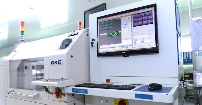
Solder Paste Inspection (SPI) is an automated process in the SMT (Surface Mount Technology) assembly line used to monitor the quality of solder paste deposited on PCB pads in real-time.
In an SMT production line, the process flow typically follows this sequence:
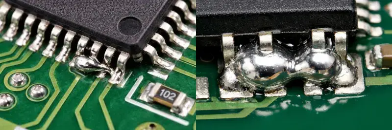
SPI is located after printing and before component placement. Specialized machines scan the printed solder paste to evaluate its geometric properties, ensuring that the volume and position of the solder paste are precise. If defects generated during the printing stage (such as insufficient solder) are not intercepted by SPI, components will be placed on an incorrect base and solidified through reflow soldering. Fixing this at a later stage requires heating, desoldering, and cleaning. This rework process is not only costly but may also damage the reliability of the circuit board.
By intercepting errors in real-time before component placement, the production line can simply wash and reprint the affected boards, thereby eliminating mass quality issues at the source.
>> Recommend reading: How to Create a Centroid (Pick and Place) File Instantly?
As electronic components evolve towards miniaturization (such as 0201 and 01005 packages) and high density (such as HDI and BGA), traditional inspection methods can no longer meet accuracy requirements.
Early 2D SPI systems used a top-down camera perspective. They primarily measured the coverage area and X/Y axis offset of the solder paste. However, 2D inspection cannot acquire height data. In actual production, even if the solder paste covers the entire pad, if the thickness is extremely thin (insufficient volume), 2D inspection will still judge it as a "Pass." However, this is highly likely to form a weak solder joint or an open circuit after reflow.
To eliminate this blind spot, NextPCB fully adopts 3D SPI technology in our production lines. Using Phase Shift Profilometry (Moiré patterns) or laser triangulation, 3D systems can reconstruct a precise three-dimensional model of the solder paste.
Its inspection dimensions include:
For BGA (Ball Grid Array) packages, the solder joints are hidden underneath the component and are difficult to observe directly after reflow. Therefore, using 3D SPI to ensure the initial solder paste volume meets specifications is the only effective preventive measure to guarantee BGA soldering reliability.
According to the IPC-7527 (Requirements for Solder Paste Printing) standard, SPI primarily monitors the following failure modes:
NextPCB treats SPI not just as a means to filter defects, but as a data source for optimizing production processes:
Our 3D SPI machines are interconnected with fully automated solder paste printers. When the SPI detects a minor trending offset in printing position (which has not yet exceeded the standard but shows signs of deterioration), the system automatically feeds compensation data back to the printer. This realizes real-time correction of printing parameters, preventing defects before they occur.
For complex projects utilizing 0.4mm pitch, HDI technology, or micro-via designs, the tolerance for solder paste volume is extremely low. 3D SPI can precisely control micron-level deposition, ensuring high-yield production for difficult, high-precision electronic products at NextPCB.
By intercepting problems at the front end of the process, we significantly reduce the need for later rework. Boards that have not undergone rework possess better thermal stability and electrical integrity. The application of SPI allows customers to obtain high-quality hardware that meets "First Pass Yield" standards in a shorter cycle.
Answer: No. While SPI is excellent at catching printing issues, post-reflow AOI (Automated Optical Inspection) detects defects that occur during placement and reflow, such as tombstoning, component shifting, polarity errors, and solder balls. SPI and AOI are complementary: SPI ensures the "foundation" is correct, while AOI ensures the "structure" is finished properly.
Answer: This is often a "False Call." Solder has a self-aligning property during reflow due to surface tension; a slight offset caught by SPI might be corrected naturally in the oven. However, at NextPCB, we maintain strict SPI thresholds because relying on "luck" during reflow compromises long-term reliability, especially for high-density BGA and 0201 components.
Answer: Traditional 2D SPI cannot, but our high-resolution 3D SPI systems use Moiré fringe technology to achieve micron-level vertical resolution. For 01005 or 0402 (metric) packages, measuring volume is more reliable than measuring height alone, as the total amount of flux and alloy determines the joint's strength.
Answer: It significantly reduces it. The closed-loop allows the SPI to tell the printer to adjust its X/Y alignment or clean the stencil automatically. However, human engineers at NextPCB still monitor the trend data to identify when a stencil needs replacement or when the solder paste viscosity is changing due to ambient temperature.
Answer: Warpage is a challenge for SPI because it changes the reference "zero" height. Advanced 3D SPI machines used by NextPCB employ "Warpage Compensation" algorithms that map the board's surface profile first, ensuring that height measurements are relative to the local pad surface, not a theoretical flat plane.
Solder Paste Inspection is not a simple visual check, but a quality assurance tool based on volumetric measurement. As circuit board design density continues to increase, the era of relying on manual or 2D inspection has passed.
By applying advanced 3D SPI technology, NextPCB ensures that the foundational step of PCBA manufacturing—solder paste printing—achieves excellence. This allows designers to focus their energy on product innovation without worrying about hidden failures in the manufacturing process.
Need high-quality PCB assembly services?

Still, need help? Contact Us: support@nextpcb.com
Need a PCB or PCBA quote? Quote now

