
 NextPCB Capabilities
Printed Circuit Boards
NextPCB Capabilities
Printed Circuit Boards
 PCB Assembly
 Layer Buildup
 SMD-Stencils
 PCB Design-Aid & Layout
 Mechanics
 Quality
 Drills & Throughplating
 Factory & Certificate
 PCB Assembly Factory Show
Certificate
PCB Assembly Factory Show
Certificate
Support Team
Feedback:
support@nextpcb.com


PCB solder mask offers protection to circuit boards during manufacturing. When circuit boards undergo fabrication, the copper traces of the board are usually exposed to environmental elements such as air and moisture, resulting in rust.
So, to protect these copper traces on the printed circuit board, thus improving it, PCB manufacturers apply solder masks to protect the circuit boards. This guide shares intriguing details regarding PCB solder mask, their types, and a step-by-step guide to applying PCB solder masks.
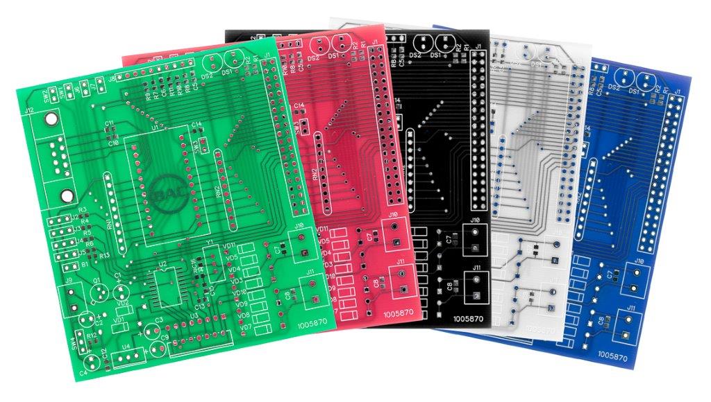
Naturally, circuit boards, upon fabrication, often appear in dull colors (grey or brown). However, with the solder mask application on the circuit board, it becomes green (or other PCB colors of choice). This process is a result of a protective layer called a solder mask.
Solder mask is a protective coating applied over the printed circuit board's surface, preventing the board's circuitry from electrical shorts and overall oxidation. The traditional color for solder masks is usually green hence why most PCBs are called green PCBs.
PCB solder mask prevents oxidation, a reaction when a metal is exposed to air in the atmosphere. During oxidation, the metal reacts with air losing its chemical properties and starting to rust. So, to prevent PCB from oxidation, applying a solder mask is crucial.
Also, Solder Mask offers protection from electrical shorts in the Printed Circuit Board. Without the solder mask application, solder paste interacts with the copper traces on the PCB during assembly. So, when components are soldered on the circuit board, there will be shorts leading to design failure.
There are four significant types of PCB solder masks used in the PCB manufacturing process. They include the following:
PCB manufacturers and engineers employ these masks to identify openings in the green solder mask, which is already applied on the printed circuit. This solder mask is applied through epoxy liquid or film methods.
After identifying the openings, components are soldered through them on the circuit boards. The solder mask used to determine top board traces is the top-side mask. Similarly, the solder mask employed in bottom board traces is called the bottom-side mask.
In terms of cost, epoxy is a cheap material for solder masks. The epoxy liquid is a polymer that hardens when heated and silkscreened on the printed circuit board.
Silkscreening is a printing technique that utilizes a mesh that identifies open areas that require inking. This process prevents the blocking of component holes on the printed circuit board.
This kind of solder mask is a combination of two different liquids. These liquids are kept separately and are usually mixed before the application of the solder mask to improve the shelf life of the printed circuit board.
LPI solder mask is available in different PCB colors, which offer differences in designs and applications across the electronic industry.
The dry film solder mask application on the PCB board uses vacuum lamination. The dry film is placed over the circuit board, and a vacuum seals the film on the PCB. Since this film is dry, it offers no film irregularities in copper plating.
Flat-printed circuit boards benefit from dry film solder masks, which offer uniform thickness. However, it is pretty expensive compared to LPI solder masks.
It is normal to think that applying a PCB solder mask is relatively easy. But it is only easy when you use a DIY Solder mask on simple design PCBs. However, PCB manufacturing and assembly is a different ball game as PCB trends usually change.
Also, PCB manufacturers require the right equipment, machines, and materials to apply a solder mask on a circuit board effectively. Here are the step-by-step processes to apply solder masks on printed circuit boards.
Before carrying out any process, the circuit boards must be thoroughly clean and free from dust and moisture.
After thorough board cleaning, the board is placed in a vertical coater containing solder mask ink coating. The ink covers the entire copper traces on the circuit board. The coat's thickness varies on the number of components and the thickness of the printed circuit board.
After coating, the next step is to place the ink-coated PCB into a dryer, where it is carefully inspected for an even and solid layer. This process also ensures that unwanted coating can be easily removed before the next stage.
Next, imaging is done by utilizing a photo film (transparent) that has circuit images fit on the printed circuit board before exposure to Ultraviolet light. During exposure, the solder mask covered by the transparent film becomes hardened. While the solder mask covered by the circuit images still maintains pre-hardening.
This process must be done with excellent precaution and preciseness by aligning the transparent film perfectly on the circuit board; otherwise, the whole PCB batch becomes obsolete.
In the Developing stages, the circuit board is put into a developer, a machine consisting of high-pressure water sprays. The developer washes away the transparent film and excess unhardened ink coating.
After the developing stage, the board undergoes hardening so that the ink coating becomes hard across the entire surface. Also, the circuit board is then cleaned to remove dust particles from its surface. After the cleaning process, the next step is surface smoothening and assembly of electrical components on the circuit board.
Solder masks are essential during PCB manufacturing and fabrication by applying a protective layer on the circuit boards to prevent oxidation and circuit shorts. Also, a solder mask ensures easy soldering of components on the circuit board without causing damage to the copper traces.
Solder masks undergo different processes to ensure that your PCB stands out in its design and application. Your PCB Manufacturer must uphold the importance of solder masks in your PCB design.
At NextPCB, we take PCB solutions and services to the next level with start-of-the-art modern manufacturing facilities. We believe in quality PCBs and seriously handle our manufacturing and assembly process with great care and precision.
Do you have a specific PCB design in mind? Try us today. Quote Now and get the best quality service.
Still, need help? Contact Us: support@nextpcb.com
Need a PCB or PCBA quote? Quote now


 Surface

