
 Surface


Lolly Zheng- Sales Account Manager at NextPCB.com

 NextPCB Capabilities
Printed Circuit Boards
NextPCB Capabilities
Printed Circuit Boards
 PCB Assembly
 Layer Buildup
 SMD-Stencils
 PCB Design-Aid & Layout
 Mechanics
 Quality
 Drills & Throughplating
 Factory & Certificate
 PCB Assembly Factory Show
Certificate
PCB Assembly Factory Show
Certificate
Support Team
Feedback:
support@nextpcb.com


Table of Contents
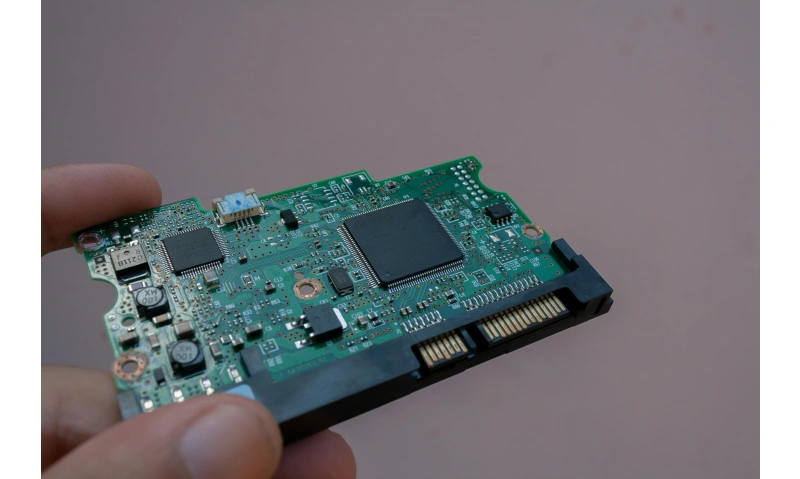
Look at any electronic device you own, from your smartphone or laptop to your coffee maker or TV. If you were to open it up, you'd find a board inside, often green (though sometimes blue, red, or black), covered in a complex network of tiny lines and metal parts. This board is the core structural element of our digital world: the PCB, or Printed Circuit Board.
So, what exactly is a PCB? Simply put, a PCB is a foundational structure that provides physical support for all the electronic components in a device and connects them electrically.
Before PCBs existed, building circuits was a messy, manual process called "point-to-point wiring." This involved connecting every component with individual wires, resulting in a system that was bulky, unreliable, difficult to repair, and inefficient to mass-produce. The PCB solved all these problems, paving the way for the reliable, compact, and affordable electronics we rely on every day.
While some high-tech boards can be incredibly complex with dozens of layers, almost all PCBs share four fundamental parts:
This is the fundamental material that gives the PCB its rigidity and structure.
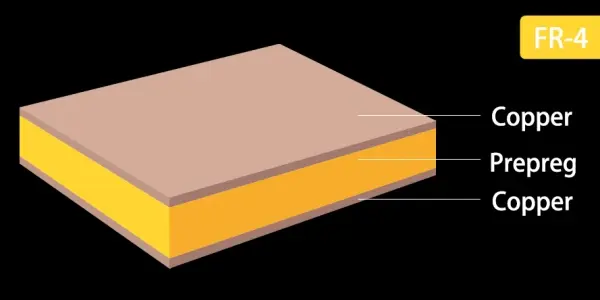
It must be mechanically strong to prevent the board from bending or breaking. The most common material is FR-4, a strong, fiberglass-reinforced epoxy resin.
The most important point: the substrate does not conduct electricity (it is an electrical insulator). This ensures that electrical current only flows through the designated conductive paths.
This is a very thin layer of conductive copper foil laminated onto one or both sides of the substrate. This forms the "Circuit" part of the Printed Circuit Board.
During manufacturing, a special etching process removes the excess copper, leaving behind only the precise, designed paths that connect the components. These conductive paths are called "Traces" (or tracks).
> Recommend reading: How Is Copper (Cu) Used in PCB Manufacturing?
This is a protective polymer layer, typically green, that covers the copper traces.
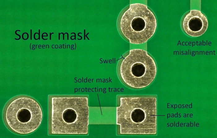
It has two crucial jobs:
This is the layer of ink, usually white, printed on top of the solder mask.
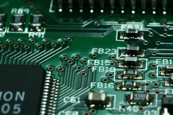
The silkscreen provides helpful reference information, such as component designators (e.g., R1, C3), company logos, component outlines, and orientation marks. This is essential for assembly, testing, and repair.
The PCB's function is clever and simple in concept:
In essence, the PCB turns a "circuit schematic" (a conceptual drawing of the circuit) into a physical, functional object that can be mass-produced.
The components are the active parts of the PCB, responsible for performing the circuit's function. They are fastened to the PCB using a process called "soldering" (where a molten metal alloy is used to create a permanent physical and electrical connection). Common components include:
The journey from an idea to a finished PCB is fascinating. It starts with engineers using specialized Computer-Aided Design (CAD) software to draw the circuit and lay out where every component goes.
To learn more about this process, from the initial schematic to the final files sent to a manufacturer, check out our in-depth guide: Printed Circuit Board Basics: From Design to Final Artwork.
The creation of a functional, multi-layer PCB requires specialized chemical and mechanical processes to connect the individual layers we just discussed. These steps are performed in a precise sequence:
1. Material Selection (The Foundation)
This crucial initial step involves choosing the right base material (substrate) for the PCB. The choice depends entirely on the application's requirements, such as the operational frequency of the circuit, the thermal resistance (Tg), and, of course, the cost. While FR-4 is the industry standard for general-purpose boards, specialized applications like high-speed wireless devices may require advanced materials like PTFE or other high-performance laminates.
>> PCB Manufacturing Process Series - Episode 1 How to Choose the Substrate Materials
2. Inner Layer Fabrication & Etching
For multi-layer boards, the copper patterns for the internal layers must be defined first. This process involves coating the copper-clad core material with a photosensitive film (photoresist), exposing it to UV light through the circuit blueprint (photomask), and chemically etching away the unwanted copper. This leaves only the precise, desired circuit traces on the inner layers.
>> PCB Manufacturing Process Series - Episode 2: Outer Layer Process
3. Lamination (Layer Stacking)
After the inner layers are patterned, they are stacked together. This involves using intense heat and pressure to bond the inner circuit layers, insulating layers called prepreg (a fiberglass-epoxy bonding sheet), and copper foil to form a single, rigid, multi-layer board.
>> PCB Manufacturing Process Series - Episode 3 Lamination
4. Drilling
Highly precise Computer Numerical Control (CNC) machines drill all the required holes into the laminated board. These holes serve two main purposes: mounting component leads and creating vias (vertical interconnect access) to allow electrical signals to pass between layers.
>> PCB Manufacturing Process Series - Episode 4: Drilling
5. Plated Through-Hole (PTH) Preparation
This is a critical step that makes the non-conductive holes drilled in the previous step capable of carrying electricity. A chemical process deposits a thin, uniform layer of copper inside the walls of the holes. This allows the signal to travel seamlessly from one copper layer to another.
>> PCB Manufacturing Process Series - Episode 5: PTH
6. Outer Circuit Fabrication Process
This process defines the final copper patterns on the top and bottom (outer) surfaces of the board. This involves:
>> PCB Manufacturing Process Series - Episode 6: Outer Circuit Fabrication Process
The simple design described above is just the beginning. To meet the demands of different technologies, PCBs come in many forms. For example, a simple toy might use a "Single-Sided Board" (only one layer of copper), while complex devices like smartphones and computers use "Multi-Layer Boards," which stack many circuit layers together to achieve high component density.
To explore this variety, please refer to our detailed post on the Types of PCBs and their specific applications.
So, what is a PCB? It is the physical backbone of almost every electronic device in existence. It is a platform for connection, a marvel of manufacturing, and the key technology that allows for the complexity and miniaturization of the modern world. Without the humble Printed Circuit Board, the high-tech gadgets we use every day simply would not be possible.
Here at NextPCB, we specialize in bringing these designs to life, manufacturing high-quality, reliable PCBs for innovators and businesses around the world.
Ready to start your next electronics project? Get an instant quote from NextPCB today!

Still, need help? Contact Us: support@nextpcb.com
Need a PCB or PCBA quote? Quote now

