
 NextPCB Capabilities
Printed Circuit Boards
NextPCB Capabilities
Printed Circuit Boards
 PCB Assembly
 Layer Buildup
 SMD-Stencils
 PCB Design-Aid & Layout
 Mechanics
 Quality
 Drills & Throughplating
 Factory & Certificate
 PCB Assembly Factory Show
Certificate
PCB Assembly Factory Show
Certificate
Support Team
Feedback:
support@nextpcb.com


Introduction: The Evolution of Prototyping
Not long ago, prototyping a printed circuit board assembly (PCBA) meant hours bent over a workbench. Engineers would manually place resistors, capacitors, and chips by hand, carefully soldering each connection with the hope that the board would function on the first try. It rarely did. Every iteration required painstaking rework, stretching development cycles into weeks or even months.
Fast forward to today, robotic arms move at blinding speed, placing components that are smaller than a grain of sand with sub-millimeter accuracy. Automated soldering stations ensure every joint is clean, while cameras powered by artificial intelligence (AI) scan for invisible defects in milliseconds. What once demanded days of labor now happens in hours, sometimes minutes.
This shift isn't just about convenience. It's about competitive edge. In modern electronics, the speed of iteration often determines who captures the market first. A McKinsey report revealed that companies leveraging effective prototyping can cut development costs by as much as 30% while accelerating time-to-market by up to 50%, a difference that can decide whether a product succeeds or becomes obsolete before launch.
The journey from manual soldering to machine intelligence is more than a tale of automation. It's the story of how humans, AI, and robotics are converging to shape the future of hardware innovation, where creativity, optimization, and precision work together rather than in isolation.
In the early days of electronics, prototyping a circuit board was closer to craftsmanship than engineering. Every component was placed by hand, every joint soldered manually, and every error had to be corrected with a desoldering pump or by starting over. This approach, while precise in skilled hands, was slow and error-prone. For a complex board, engineers could spend several days just assembling a single prototype, with no guarantee it would work as intended.
The first wave of transformation came with robot-assisted processes. Pick-and-place machines revolutionized assembly by automating the most time-consuming step, component placement. Instead of a human placing perhaps 200–400 components per hour, a modern high-speed pick-and-place system can mount 30,000 to 50,000 components per hour with a placement accuracy of ±0.01 mm. For reference, that's the thickness of a human hair divided by ten.
Next came the integration of reflow ovens and automated soldering systems. These ensured uniform heating and bonding across hundreds of solder joints simultaneously, drastically reducing weak connections that plagued manual prototypes. In fact, studies have shown that automated soldering can reduce defect rates by 30–40% compared to manual processes.
The cumulative effect of these advancements has been a fundamental change in the way engineers work. Instead of spending hours placing and soldering, they can now focus on design, testing, and innovation. Robotics handles the repetitive, heavy lifting, freeing human expertise for higher-level problem-solving.
But even with robotics, one challenge remained. That is quality control. Machines could assemble boards quickly, but identifying subtle defects, such as hairline solder cracks or misaligned microcomponents, still relied heavily on human inspectors. That limitation paved the way for AI to enter the picture.
While robotics brought speed and consistency to PCBA prototyping, the question of accuracy and foresight remained. Machines could place thousands of components per hour, but even the most advanced robotic system was only as good as the rules it was programmed with. Subtle defects often slipped through, and predicting design flaws before a board was even built was beyond their capability. This is where artificial intelligence (AI) has become indispensable.
Modern Automated Optical Inspection (AOI) systems, enhanced with machine learning, have dramatically improved defect detection. High-resolution cameras capture images of every solder joint and component, while AI models, trained on thousands of defect patterns, instantly flag issues such as solder bridges, misalignments, and micro-cracks invisible to the naked eye.
Beyond defect detection, AI is transforming design validation. By simulating how heat, signals, or stress will flow across a board, AI tools can predict problems before fabrication even begins. For example:
This predictive layer is a game-changer. Instead of waiting days for a prototype only to discover a design flaw, engineers can catch and fix errors in hours. Integrating AI-driven design-for-manufacturing (DFM) checks can shorten the prototype iteration cycle by 30–40%. In short, AI doesn't replace the engineer; it acts as a second pair of eyes with superhuman speed and accuracy. Robotics builds faster, but AI ensures smarter, more reliable outcomes.
The future of PCBA prototyping isn't a competition between humans and machines — it's a partnership. Each plays a role that the others cannot replace, and together they create a workflow that is faster, smarter, and far more reliable.
Engineers define the purpose of the design. They ask what problem this circuit should solve. How should it interact with users or other systems? Their strengths include system-level thinking, where they decide functionality, power requirements, and connectivity. They also apply creativity and intuition to solve unique design challenges. They adapt designs for new use cases that machines can't “imagine.” For instance, an engineer conceptualizes a PCB for a medical device that must monitor blood oxygen, transmit data wirelessly, and run for 48 hours on a single charge. No AI or robot can originate that vision.
AI plays a crucial role in modern PCB design. They ensure that circuits are not only functional but also manufacturable, reliable, and efficient, handling complexities that are beyond manual computation. Its strengths are evident across several critical areas. Machine learning models can predict defects by scanning layouts for potential soldering or routing issues before fabrication begins. Thermal simulations forecast hotspots and manage heat dissipation to prevent failures. Signal integrity checks identify risks like crosstalk in high-speed circuits, a common cause of prototype breakdowns. Also, AI optimizes yields by predicting production outcomes, which improves first-pass success rates. Notably, AI-driven design-for-manufacturing (DFM) checks have been shown to cut design-related errors by 30–40%, leading to a significant reduction in costly re-spins.
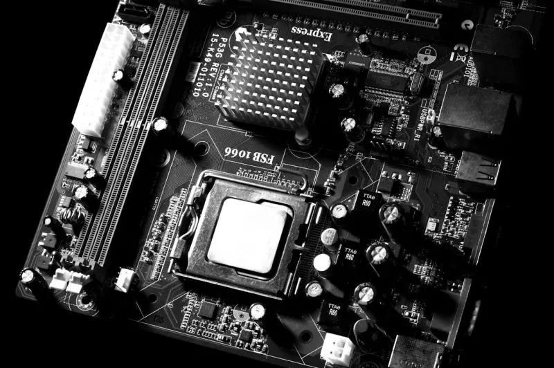
Robotics takes optimized PCB designs and brings them into physical reality at a speed and precision far beyond human capability. Pick-and-place machines, for example, can mount 30,000–50,000 components per hour with an accuracy of ±0.01 mm, enabling the rapid assembly of even the most complex boards. Automated soldering systems ensure consistent quality across thousands of joints, minimizing the risk of weak connections, while robotic inspection systems integrated with automated optical inspection (AOI) guarantee accuracy in both placement and soldering. A striking example is seen in smartwatch PCBs, often smaller than a coin, where robotics can seamlessly place MEMS sensors, microcontrollers, and antenna components so tiny and intricate that manual assembly would be virtually impossible.
For example, a wearable health tracker:
NextPCB is one of the manufacturers already embodying the full integration of human expertise, AI-driven optimization, and robotics/automation. Their capabilities show how the theoretical collaboration becomes real in everyday PCBA prototyping and production.
Here are bullet points with verified details about what NextPCB offers, based on the latest public data:
NextPCB operates at a remarkable scale, with two dedicated PCB manufacturing plants and two PCB assembly factories covering a combined footprint of over 20,000 square meters. The company runs 36 fully automated Siemens Surface Mount Technology (SMT) lines, enabling high-speed and high-precision production. In terms of output, NEXTPCB's facilities achieve a daily capacity of more than 95 million solder joints in assembly, underscoring both its efficiency and ability to handle large-volume orders with consistent quality.
NextPCB maintains a strong commitment to quality and compliance, backed by internationally recognized certifications and standards. The company is certified under ISO 9001 for quality management, IATF 16949 for automotive manufacturing, and ISO 13485 for medical device production, ensuring sector-specific reliability and precision. All boards undergo inspection aligned with IPC-A-600 and IPC-A-610 standards, with Class 2 provided as the default and Class 3 available for high-reliability applications. In addition, NEXTPCB holds RoHS, REACH, and UL certifications, guaranteeing product safety, strict control of hazardous substances, and compliance with global regulatory requirements.
NextPCB offers a full spectrum of PCB manufacturing solutions, ranging from quick-turn prototypes to complex 32-layer boards, including HDI, rigid-flex, metal-core, and high-frequency designs. Their advanced fabrication supports fine-pitch components, handling as small as 0.25 mm pitch BGA/QFN packages and miniature passives like 01005/0402 resistors, enabling the development of next-generation compact and high-performance electronics.
> PCB Assembly Capabilities | Quick-Turn Prototype to Volume Production
At NextPCB, quality control is comprehensive and precise. AOI (Automated Optical Inspection), in both 2D and 3D, is used to inspect solder paste, component placement, reflow, and final assemblies, with 3D AOI providing height and volume measurements to detect hidden defects. X-ray inspection, including AXI, allows for the examination of hidden solder joints, such as those under BGAs, as well as internal layer alignment issues. Electrical testing is equally thorough, with bare-board E-tests, flying probe tests, and in-circuit testing (ICT) used to identify opens, shorts, and internal trace defects, ensuring that every PCB meets stringent quality standards.
> PCB/PCBA Test Methods by Category
NEXTPCB provides free Design for Manufacturability (DFM) and Design for Assembly (DFA) checks, where engineers carefully review designs to identify potential issues before fabrication, helping to prevent costly errors. Additionally, online tools such as a Gerber viewer and real-time BOM (Bill of Materials) sourcing leverage a large global inventory to manage part lead times and suggest alternative components, streamlining the design-to-production process.
NEXTPCB offers rapid prototype deliveries. Every great company knows speed is a major advantage. For instance, prototypes of 1–2 layer boards can be manufactured in as little as 24 hours, and the company offers free functional testing on up to 10 prototype units. This rapid turnaround allows startups and R&D teams to move through design iterations quickly and confidently, knowing their boards are both tested and production-ready.
> Turnkey PCB Assembly Services | China PCB Manufacturer - NextPCB
Using these capabilities, here's how NextPCB puts the collaboration into practice:
|
|
|
|
|
|
|
|
|
|
|
|
|
|
|
|
Imagine an R&D team designing a next-generation wearable device. Here's how the collaboration with NextPCB typically unfolds:
Step 1: Submit Your Manufacturing Files
You upload the key documents required for assembly, Gerber files, bill of materials (BOM), and pick-and-place (centroid) files. These files contain all the data needed for fabrication and assembly, without requiring you to hand over your full design source files. This protects your IP while giving NextPCB everything necessary to begin.
Step 2: Automated DFM/DFA Review
Before fabrication begins, NextPCB performs a Design for Manufacturability (DFM) and Design for Assembly (DFA) review. This process flags issues such as incorrect trace widths, insufficient copper spacing, or components placed too close to one another. By resolving these upfront, you avoid costly redesigns and delays later in the process.
Step 3: Component Sourcing
NextPCB's sourcing team checks the BOM against their inventory of over 600,000 in-stock parts and their trusted supplier network. If a component is unavailable, they recommend suitable alternatives before production begins. This step ensures your build doesn't stall due to supply chain gaps.
Step 4: Prototyping and Assembly
Once the files are cleared and components confirmed, production begins. Robotic pick-and-place machines assemble components with ±0.01 mm accuracy, followed by reflow soldering for consistent joints. For small prototype runs, technicians often step in to assist, ensuring flexibility and attention to detail.
Step 5: Inspection and Testing
In volume production, boards are inspected using 2D Automated Optical Inspection (AOI) and X-ray testing, which help identify hidden defects such as voids under BGAs. For prototype runs, inspection is typically performed by skilled technicians, with any issues corrected before boards are shipped. Customers can also request functional testing, and NextPCB offers this service free for up to 10 prototype units—so teams can validate core functionality before scaling.
Step 6: A Working Prototype in Hand
The result is a high-quality prototype delivered faster and with fewer surprises. By combining early design checks, intelligent sourcing, precision assembly, and careful inspection, NextPCB ensures your design moves from digital files to reliable hardware seamlessly.
Reduced iteration cycles: Because designs are checked early, errors are caught earlier, and you can save potentially 30-40% of time that would otherwise go into redesigns or debugging.
NextPCB doesn't just offer tools. It embodies the hybrid approach you need in modern PCBA prototyping.
The story of PCBA prototyping has moved far beyond the era of manual soldering and trial-and-error assembly. Today, we stand in a new phase where engineers, AI, and robotics form a powerful triad, each contributing creativity, intelligence, and precision. Engineers bring the imagination and problem-solving mindset, AI optimizes complex systems at speeds no human could match, and robotics executes with repeatability and accuracy down to microns.
This collaboration isn't just theoretical. It's reshaping industries in real time. Companies that embrace this model are already seeing shorter development cycles, higher first-pass success rates, and faster entry to market. For startups, this can mean survival. For established enterprises, it can mean leadership in a fiercely competitive space.
Yet, the future is not about machines replacing humans. It is about machines amplifying human creativity, removing the bottlenecks of time, error, and scale so that ideas can move from whiteboards to working prototypes faster than ever before. As autonomous prototyping and smarter AI-driven simulations continue to evolve, human ingenuity will remain the compass guiding technology forward.
Manufacturers like NextPCB show how this vision is already possible today. By combining skilled engineers, intelligent inspection systems, and robotic assembly lines, they act as the bridge that makes human and machine collaboration a practical reality for innovators worldwide. The message is clear. The future of PCBA prototyping is collaborative. Those who align with this human, AI, robotics partnership will not just keep up with innovation, they will set its pace.
About the Author
Abiola Ayodele: Broadcast Journalist & Tech Writer; Cooperate writer of NextPCB.
Specialize in technical writing, and editing, particularly in the areas of PCB design, semiconductors, cybersecurity, and emerging engineering technologies.
Still, need help? Contact Us: support@nextpcb.com
Need a PCB or PCBA quote? Quote now


 Surface

