

 Surface


Julia Wu - Senior Sales Engineer at NextPCB.com

 NextPCB Capabilities
Printed Circuit Boards
NextPCB Capabilities
Printed Circuit Boards
 PCB Assembly
 Layer Buildup
 SMD-Stencils
 PCB Design-Aid & Layout
 Mechanics
 Quality
 Drills & Throughplating
 Factory & Certificate
 PCB Assembly Factory Show
Certificate
PCB Assembly Factory Show
Certificate

Support Team
Feedback:
support@nextpcb.com


In the last piece, we looked at how AI server demand is driving up PCB prices industry-wide. One number from that piece is worth pulling apart on its own: an AI server's PCB can be worth over three times what a conventional server's PCB is worth. Most of that gap comes down to one thing — the board inside an AI server isn't just a bigger version of a standard board, it's a different class of manufacturing problem, and the biggest single driver of that is layer count.
This piece breaks down what a "high-multilayer compute board" actually is, why adding layers doesn't scale in cost the way people assume, and where the money actually goes.
A standard commercial PCB — the kind in a router, a consumer gadget, an industrial controller — typically runs 4 to 10 layers. A conventional server motherboard runs higher, often 12 to 16 layers, to handle DDR5 memory channels and PCIe lanes. An AI server baseboard hosting GPUs like NVIDIA's H100 or B200 is a different tier entirely.
| Board type | Typical layer count | Via technology |
|---|---|---|
| Standard commercial PCB | 4–10 layers | Mechanically drilled through-holes |
| Conventional server motherboard | 12–16 layers | Through-holes, limited HDI |
| AI server CPU/networking board | 16–24 layers | HDI with blind/buried vias |
| AI GPU baseboard / OAM module | 20–32+ layers | Laser-drilled microvias, stacked/staggered structures |
| Specialized inspection/testing boards | Up to 100+ layers | Ultra-thin material, precision handling |
(Compiled from multiple manufacturer and industry technical sources; exact layer counts vary by GPU generation and board function.)
The reason AI GPU baseboards need this many layers comes down to pin density. A modern AI accelerator package can carry 5,000 to 8,000+ pins at sub-1mm pitch. Routing power and thousands of high-speed differential pairs — for interconnects like NVLink and PCIe Gen5/6 — out of that footprint without layers to spare simply isn't possible on a board with a dozen layers. For a deeper technical walkthrough of this specific problem, see NextPCB's HDI PCB for AI Servers: Stackup, Via-in-Pad & Laser Drill Guide.
Here's the part that surprises people outside the industry: a 30-layer board isn't built the same way as a 10-layer board, just with more steps. Past a certain layer count, a board physically cannot be built in a single lamination press cycle — the alignment accuracy required across that many copper layers exceeds what one press cycle can reliably hold.
Instead, manufacturers use sequential lamination: build a core, laminate it, laser-drill microvias into it, plate them, then laminate another set of build-up layers on top, and repeat. A 30+ layer AI GPU board typically requires 3 to 5 (and in some designs 7+) separate press cycles. Each additional cycle adds direct cost and 2–3 days of lead time, and a board that needs 4 cycles instead of 3 can cost roughly a third more even when the raw material is identical — the extra cost is entirely process complexity, not material.
Via count tells the same story from a different angle. A standard 14-layer board might use 5,000 to 12,000 through-hole vias. A 30-layer AI HDI board can carry over 100,000 microvias on a single panel, arranged in stacked and staggered configurations that have to be laser-drilled and plated with far tighter tolerances than a mechanically drilled hole.
Layer count and lamination cycles explain the process cost. What often gets left out of a per-board quote is yield — and at this complexity level, yield is not a rounding error.
A fabricator running a 28-layer ultra-low-loss board at a 75% first-pass yield is scrapping roughly one in four boards, and each scrapped board carries the full material and labor cost already sunk into it. On boards valued at four figures apiece, that scrap rate becomes a real line item — and it's a cost that shows up as a higher quoted price (or a lower margin for a fabricator who under-quotes it), rather than as a separate charge a buyer can easily see.
This is also why AI server PCB fabrication is concentrated among a small number of manufacturers rather than being broadly available. The capital equipment alone — laser drilling systems, sequential lamination presses, the metrology to hold ±5% impedance tolerance instead of the ±10% typical of standard boards — represents a multi-million-dollar investment, and reaching a workable yield on top of that equipment takes years of accumulated process control, not just the hardware.
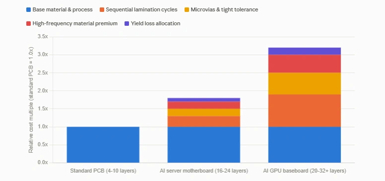
Layer count and process complexity are one axis of cost. Material grade is the other, and the two compound rather than add. AI server signal layers running NVLink or PCIe Gen5/6 at high data rates need ultra-low-loss laminates — materials like Megtron 6/7 or Tachyon 100G — instead of standard FR-4, because ordinary laminate simply can't preserve signal integrity at these frequencies over any meaningful trace length. These materials, combined with the ultra-smooth HVLP copper foil needed to keep signal loss down, can cost several times what standard FR-4 and copper cost per panel. NextPCB's guide to High-Speed PCB Materials for AI Servers goes through how these material choices map to specific interconnect requirements.
Put together — layer count, sequential lamination, microvia density, yield loss, and premium materials — industry cost breakdowns generally attribute roughly 80% of an AI server board's total cost to these five factors combined, rather than any single one of them being the whole story.
If your project is heading toward a 20-layer-plus HDI stackup, the practical takeaway is that layer count alone doesn't tell you what you'll pay — the lamination cycle count, via structure, material grade, and impedance tolerance you specify all move the price independently of each other, and they interact. NextPCB's AI Server PCB Design Checklist and Server Motherboard PCB Manufacturing guide both go deeper into the specific stackup and reliability decisions that drive this.
Working on a stackup in this range and want a real number instead of a rule of thumb? Upload your design to NextPCB's online quote and order page — for high-layer-count and HDI boards, you'll get engineering-reviewed pricing that reflects your actual stackup, not a generic per-layer estimate.
It depends on the board's role. AI server motherboards typically run 16 to 24 layers, while the GPU baseboards and OAM modules that carry the accelerator packages themselves commonly need 20 to 32+ layers. Some specialized boards, like those used in semiconductor test equipment, have pushed past 100 layers. The driving factor is pin density on the package being routed, not a fixed industry number.
HDI boards aren't just "more layers" — they use laser-drilled microvias, sequential lamination in multiple press cycles, and tighter impedance and registration tolerances than a standard through-hole multilayer board. Industry pricing generally puts HDI boards at 50–200% more expensive than standard PCBs at equivalent layer counts, because the premium reflects process complexity and yield risk, not just extra copper and prepreg.
It's a real and often underestimated factor. A fabricator without mature process control on a 28-layer ultra-low-loss board can see first-pass yield in the 70–80% range, meaning a meaningful share of boards are scrapped after most of the material and labor cost has already gone into them. That risk gets priced in — either explicitly in the quote, or as a hidden cost that shows up later as inconsistent quality from an under-equipped supplier.
Not every fabricator can. Sequential HDI lamination requires laser drilling equipment, multi-cycle press capability, and metrology for tight impedance control that a shop focused on standard 2–10 layer boards typically doesn't have. Before committing a design to a supplier, it's worth confirming their specific capability at the layer count and material grade you need, rather than assuming general PCB manufacturing experience carries over.

Still, need help? Contact Us: support@nextpcb.com
Need a PCB or PCBA quote? Quote now

