
 Surface


Zhang

 NextPCB Capabilities
Printed Circuit Boards
NextPCB Capabilities
Printed Circuit Boards
 PCB Assembly
 Layer Buildup
 SMD-Stencils
 PCB Design-Aid & Layout
 Mechanics
 Quality
 Drills & Throughplating
 Factory & Certificate
 PCB Assembly Factory Show
Certificate
PCB Assembly Factory Show
Certificate
Support Team
Feedback:
support@nextpcb.com


Table of Contents
Modern electronic system design faces unprecedented demands for power density, driven by the trend toward smaller sizes, higher integration, and stable operation in increasingly harsh environments. In this context, the limitations of traditional FR4 PCBs in terms of thermal management design are becoming increasingly evident. Their low thermal conductivity (typically less than 1 W/(m·K)) makes them a bottleneck for system heat dissipation. For high-power applications requiring conduction cooling, heat must be efficiently conducted laterally from the heat-generating components to the cold plate edges. This makes the PCB plane's lateral thermal conductivity crucial.
The Aluminum Core PCB (Metal Core PCB, MCPCB) is a key technology developed precisely to solve this challenge. The core concept of MCPCB is to replace the bulk of the low-conductivity insulating substrate with a highly conductive metal core (such as aluminum or copper), providing a low-impedance path for heat flow. This structure significantly enhances the in-plane thermal spreading capability of the PCB, making it a standard solution in fields such as high-power semiconductors and LED lighting.
This engineering case study focuses on an advanced thermal management structure: a double-sided component mounted PCB featuring an aluminum heat-dissipation core. This design utilizes Surface Mount Technology (SMT) for flat-pack integrated circuits installed on thin circuit layers, which are then bonded to both sides of the central aluminum plate (refer to descriptive Figure 12-8). The goal is to maximize power handling capacity. The design target is to maintain a minimal temperature rise under a total dissipation power of 4.8 W through efficient conduction cooling. Through rigorous engineering calculations and thermodynamic analysis, this article quantifies the thermal performance of this design and discusses its value and limitations in practical applications.
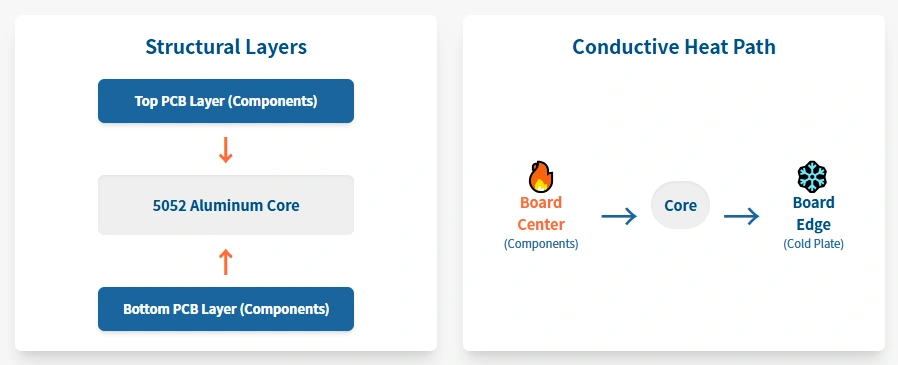
The aluminum core PCB structure shown in this case represents an advanced design form for high power density applications. It consists of three main functional layers: thin circuit layers on both sides (including dielectric insulation and copper traces), and the highly conductive aluminum core in the middle. Components are mounted on the thin circuit layers using Surface Mount Technology (SMT). This double-sided mounting structure significantly increases system integration.
Due to the aluminum core's excellent thermal spreading capability, this structure can accommodate twice as many integrated circuit components as a PCB with components on only one side, resulting in a total dissipation power double that of a single-sided PCB. In this case, electronic components are mounted on both sides of the board, with 2.4 W of power dissipated by components on each side, totaling 4.8 W for the entire PCB. This design strategy not only addresses space constraints but, more importantly, leverages the symmetric and efficient heat conduction characteristics of the metal core. You can find more details in PCB Thermal Design Basics (1): Substrate Material Selection.
Achieving this complex double-sided bonding structure places high demands on lamination and thermal interface processing. The quality of the bond between the thin circuit layers and the aluminum core directly determines the vertical thermal resistance of heat flow from the component to the metal core. Manufacturing highly reliable multilayer metal core PCBs requires precise control over the thickness and composition of the thin dielectric material and ensuring the integrity of the bonding interface. For example, NextPCB specializes in manufacturing high-reliability metal core PCBs (MCPCBs), offering high-quality lamination processes that ensure low thermal resistance and long-term reliability of the thermal interface material, which is crucial for achieving the efficient 4.8 W heat dissipation target outlined in this case.
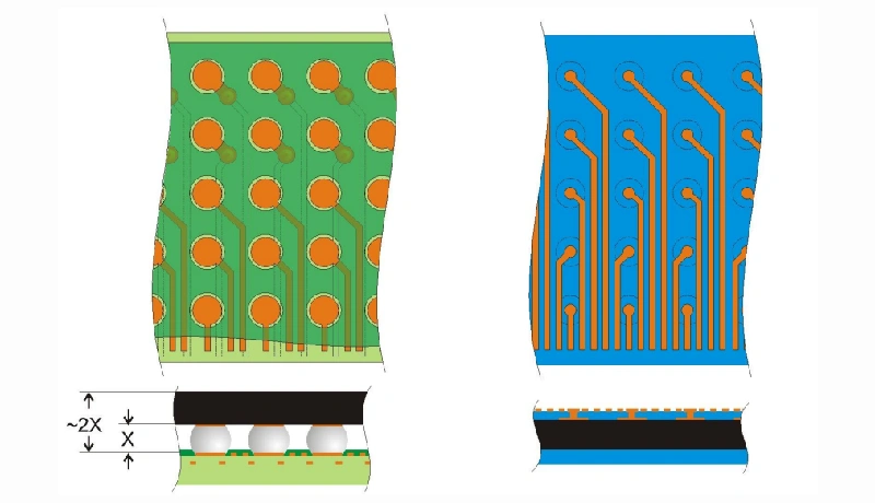
Figure II. Schematic diagram of a sequential manufacturing or assembly process.
Source: Reprinted from “Occupational Exposure to Carbon Nanotubes and Nanofibers,” by the National Institute for Occupational Safety and Health (NIOSH), 2013.
A key thermodynamic advantage of this design lies in its symmetry and uniform component distribution. If all components have roughly the same power dissipation, the aluminum core PCB will generate a uniform thermal load. This uniform thermal load is the basis for simplified engineering analysis.
In a conduction-cooled PCB, heat flows from the center toward the cooled edges. When the thermal load is uniform, heat conduction across the board follows the classical one-dimensional (1D) conduction model, with a parabolic temperature rise distribution (refer to descriptive Figure II.B.). This means the highest temperature is located at the geometric center of the board (the point with the longest heat flow path), and the lowest temperature is at the edges contacting the system-level cold plate.
This structural symmetry ensures thermal efficiency: although the total power is 4.8 W, the heat is symmetrically split into two paths, 2.4 W per side, flowing uniformly from the center toward both edges. This bidirectional, symmetric heat conduction fundamentally reduces the lateral thermal resistance. By employing sound (i.e., high thermal conductivity) thermal design, the aluminum and copper heat spreaders within the board can conduct a significant amount of heat. Due to the small temperature rise, this design is particularly suitable for high-ambient-temperature environments or applications with stringent reliability requirements.
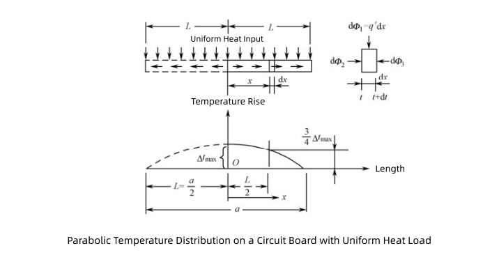
Figure II.B. Parabolic Temperature Distribution on a Circuit Board with Uniform Heat Load
Source: Adapted from "PCB Design Technology and Practice" (4th ed.), by Zhiwei Huang, 2024, Publishing House of Electronics Industry.
In high-power PCBs, conduction cooling is central, meaning heat transfer occurs primarily through solid media (copper traces, dielectric layers, and the metal core), rather than relying on less efficient convection or radiation.
For the conduction-cooled PCB shown in this case, the heat flow path can be clearly broken down into two stages (refer to descriptive Figure 12-9):
The focus of this case is precisely the performance of the aluminum core as a "lateral heat conductor" in the second stage.
To quantify the lateral conduction efficiency of the aluminum core, we use the maximum temperature rise equation (Equation 12-3) for a conduction-cooled flat plate. This equation is derived based on a 1D steady-state heat transfer model, applicable to elongated boards with a uniform heat source and ideal isothermal cooling at the edges.
Δtmax = ΦL / (2λA)
This equation calculates the maximum temperature difference (Δtmax) between the center point of the aluminum core and the edges (the cold plate contact points). A precise interpretation of the physical meaning of its parameters is key to ensuring calculation accuracy:
The essence of this formula is the result of integrating all differential thermal resistances along the length L/2. The design rationale is that the designer successfully constructed a low-lateral-thermal-resistance channel by selecting a high λ and a sufficiently large cross-sectional area A, thereby minimizing the temperature rise.
The input parameters used for this calculation are summarized below:
| Parameter (Symbol) | Physical Quantity | Value (SI Unit) | Engineering Unit | Engineering Significance |
|---|---|---|---|---|
| Φ | Single-side Dissipation Power | 2.4 W | 2.4 W | Heat flow input quantity |
| L | Total Spreader Length | 0.0762 m | 76.2 mm | Maximum conduction distance (L/2) |
| λ | 5052 Aluminum Core Thermal Conductivity | 144 W/(m·K) | 144 W/(m·K) | Determines lateral conduction efficiency |
| A | Aluminum Core Cross-sectional Area | 1.032 × 10⁻⁴ m2 | 103.2 mm2 | Size of the heat conduction channel |
According to the parameters and formula above, we can now precisely calculate the maximum temperature rise within the aluminum core (center point relative to the edge cold plate) under a total dissipation power of 4.8 W:
Substituting the known data into Equation:
Δtmax = ΦL / (2λA)
Δtmax = (2.4 W) × (0.0762 m) / (2 × (144 W/(m·K)) × (1.032 × 10⁻⁴ m2))
Δtmax = 0.18288 / 0.0297216 K
Δtmax ≈ 6.152 K
The calculated result of 6.15 K holds significant engineering value. On a board 76.2 mm long, supporting a high-power load of 4.8 W, the aluminum core material introduces a maximum temperature difference of only approximately 6.15 K. This result strongly confirms the excellent performance of the aluminum heat spreader as a lateral heat conductor. For details on other related thermal design cases, please refer to PCB Thermal Design Case Study: Copper Thickness for Uniform Heat Load.
This extremely low lateral temperature rise directly validates the effectiveness of high-conductivity materials in suppressing the in-plane thermal resistance of heat flow. Designers successfully conducted heat rapidly from the board center to the edges by increasing the thermal conductivity λ and the cross-sectional area A.
| Design/Thermal Performance Indicator | Core Value | Engineering Significance |
|---|---|---|
| Total Dissipation Power Ptotal | 4.8 W | Basis for high-density application |
| Spreader Material λ | 5052 Aluminum (144 W/(m·K)) | Optimal balance of cost and performance |
| Max Δtmax (Core) | ≈6.15 K | Extremely low lateral thermal resistance; successful conduction cooling design |
| Key Applicability Metric | Low Temperature Rise | Especially suitable for high ambient temperature or mission-critical reliability applications |
In thermal management, a small temperature rise is a key indicator of high reliability. A low Δtmax means the core center temperature is only 6.15 K higher than the edge cold plate temperature. This result leaves sufficient engineering margin for system design. For example, even if the edge cold plate temperature (Ts) reaches 85°C due to environmental factors, the aluminum core center temperature would only be 91.15°C. This makes it easier to keep the junction temperature (Tj) of the components above within the maximum safe temperature specified by semiconductor manufacturers.
Furthermore, because aluminum has a relatively high heat capacity, such a low temperature difference also suggests that the structure has higher stability against transient thermal shock, effectively smoothing out local and temporary temperature peaks. If the 5052 aluminum core (λ=144 W/(m·K)) were replaced with a high-performance pure copper core (λ ≈ 398 W/(m·K)), the theoretical temperature rise could be reduced to approximately 2.2 K. However, a Δtmax of 6.15 K is sufficiently excellent for most applications, making the 5052 aluminum core the optimal economic choice for achieving this thermal performance budget when considering the trade-off between cost, weight, and manufacturing complexity.
While the calculated result of 6.15 K is encouraging, the warning provided in the case must be strictly adhered to:
This calculation result does not include the temperature rise of the thin circuit layer and is only applicable to the aluminum core heat spreader. This marks a critical distinction in engineering analysis.
In practical high-power designs, the most important thermal metric is the component junction temperature (Tj). The system's total temperature rise (ΔTtotal) is the sum of the temperature rises generated by all serial thermal resistances from the component junction to the external cold plate (Ts):
ΔTtotal = Δtpackage + Δtinterface + Δtdielectric + Δtmax (core)
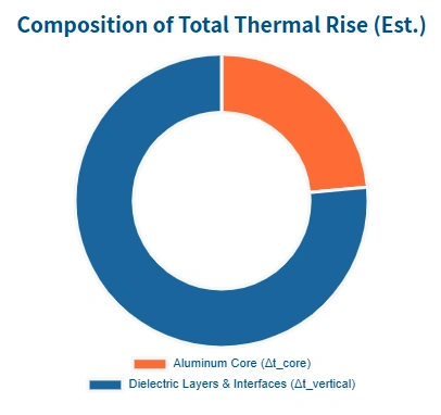
Since we have verified that Δtmax (core) is extremely low (only 6.15 K), this indicates that lateral thermal resistance is no longer the primary bottleneck. Therefore, the design focus must shift to vertical thermal resistance, particularly the thermal resistance of the thin dielectric insulating material (Δtdielectric).
When heat flows from the component junction to the aluminum core, it must pass vertically through the dielectric layer. Although the dielectric layer is extremely thin (typically between 50 μm and 200 μm), its thermal conductivity (λ) is significantly lower than that of the metal core. Even for high-performance thermal polymer dielectrics, their thermal conductivity is usually only between 3 W/(m·K) and 9 W/(m·K). This vertical heat flow bottleneck means that the dielectric layer's thermal resistance Rth, dielectric often becomes the dominant contributor to the total thermal resistance in the MCPCB structure. It is widely accepted in the industry that the thermal resistance of the dielectric layer is one of the most critical factors affecting the overall thermal performance of MCPCBs, potentially surpassing the importance of the metal base itself.
Assuming a high-performance dielectric layer provides a thermal resistance of 0.8 K/W, for a single-side power dissipation of 2.4 W, the temperature rise Δtdielectric generated by the dielectric layer alone could be 2.4 W × 0.8 K/W = 1.92 K. While this may appear lower than the core's lateral temperature rise on a macroscopic view, heat flow is highly concentrated in the local solder pad area of high-power components, making the localized dielectric thermal resistance the critical factor controlling the component junction temperature.
Because the aluminum core's lateral conduction successfully suppresses Δtmax (core) so effectively, design optimization to control and minimize Rth, dielectric becomes even more crucial. The core of MCPCB design optimization lies in selecting high-conductivity dielectric materials and using the thinnest possible dielectric layer thickness while meeting electrical insulation requirements (such as voltage breakdown). This is a key area of trade-off that electrical engineers and thermal management experts must consider, as detailed in PCB Thermal Design Basics (3): PCB Wiring Layout.
In practical design, engineers must shift their focus from "Is the board hot?" (macroscopic lateral temperature rise) to "Is the component junction temperature too high?" (microscopic vertical temperature rise). The 6.15 K core temperature difference is an indicator of the structure's successful thermal spreading, while the junction temperature Tj is the ultimate metric for reliability.
In addition to the selection and thickness control of the dielectric layer, engineers must also consider thermomechanical stress. Differences in the Coefficient of Thermal Expansion (CTE) exist between the aluminum core, the dielectric layer, and the copper foil. In applications with high thermal cycling or extreme temperature variations, this CTE mismatch can lead to delamination between layers or fatigue failure in component solder joints. Therefore, high-quality bonding processes and the selection of thermal interface materials are necessary to mitigate these stresses.
Regarding component placement, the thermal load should be distributed as uniformly as possible, and it must be ensured that high-power components have the largest possible vertical heat conduction channel beneath them. This aligns with the principles of Component Layout design, although the uniform thermal load assumption in this case has already simplified this challenge.
The success of theoretical thermal design, such as the low Δtmax demonstrated in this case, must ultimately be supported by high-quality manufacturing processes. After the lateral conduction problem is solved, controlling vertical thermal resistance becomes the key to achieving a low junction temperature, and this relies entirely on manufacturing capability.
NextPCB possesses the professional technology and equipment in the field of metal core PCB manufacturing to translate theoretical thermal performance into highly reliable, practical products.
Learn Detailed PCB Manufacturing Processes at NextPCB Factory
Beyond basic manufacturing, NextPCB also provides engineering support throughout the design and mass production phases, helping customers address complex conduction cooling challenges.
Upload & Quote Online Learn PCB Assembly Services at NextPCB
Design engineers can utilize the NextPCB engineering team to assist with more complex 3D thermal simulations. While the 1D model provided a baseline Δtmax estimate for this case, 3D Finite Element Analysis (FEA) can more accurately evaluate the thermal resistance contributions of the dielectric layer, localized hotspots, and component packages, thereby validating the assumptions of the 1D model and optimizing the layout.
NextPCB offers customized high-power solutions that can accommodate the conduction cooling interface requirements shown in this case, ensuring a tight, low-thermal-resistance connection between the PCB edges and the system-level cold plate. This comprehensive service tightly integrates theoretical thermal design with practical manufacturing capabilities, providing a solid foundation for the successful implementation of client projects.
> PCB Assembly Capabilities | Quick-Turn Prototype to Volume Production
This engineering case study provided a rigorous analysis and quantitative calculation of the thermal design for an aluminum core PCB. The analysis showed that by using a 5052 aluminum core with a thermal conductivity of 144 W/(m·K) and employing a double-sided component and symmetric conduction structure, the maximum lateral temperature rise of the aluminum core under a total power dissipation of 4.8 W was successfully limited to approximately 6.15 K.
This result strongly affirms the critical role of high-conductivity metal cores in conduction cooling applications and verifies the significant advantage of this double-sided, uniform thermal load design form in achieving high power density and high reliability. Since lateral thermal resistance has been effectively suppressed, the design focus must shift to the vertical thermal resistance between the components and the aluminum core—namely, the thermal resistance of the dielectric layer. Minimizing Rth, dielectric becomes the determining factor in ensuring the component junction temperature remains below the safety threshold.
For design engineers aiming for high performance and high reliability in high power density applications, the success of theoretical analysis must be supported by manufacturing precision. Therefore, selecting a partner like NextPCB, which offers professional capabilities and engineering support in metal core PCB manufacturing, precision dielectric layer control, and structural reliability verification, is key to translating theoretical thermal design into stable, high-performance physical products. By combining advanced thermal design principles with cutting-edge manufacturing technology, the growing heat dissipation challenges of modern electronic systems can be effectively addressed.

Still, need help? Contact Us: support@nextpcb.com
Need a PCB or PCBA quote? Quote now

