HDI PCB Manufacturer | High-Density Interconnect Manufacturing - NextPCB
NextPCB is an IATF 16949:2016 and ISO 9001 certified PCB manufacturer, operating two dedicated manufacturing facilities with a combined monthly capacity exceeding 140,000 square meters. Our engineering team of specialists supports HDI builds up to 32 layers with IPC Class 3 process control — from prototype through mass production.
Whether your project requires automotive-grade traceability (IATF 16949), medical-grade quality systems (ISO 13485), or RoHS/REACH compliance for global markets, our manufacturing processes are built to support high-reliability HDI applications across automotive, medical, industrial, and RF/telecom sectors.

- Have a complex HDI project?
- Talk to our engineering team about your stackup, layer count, and application requirements before you commit to a quote.
- >> [Schedule an Engineering Consultation]
HDI Manufacturing at a Glance
| Specification |
Capability |
| HDI Structures |
Class I, II, III — including any-layer HDI via Advanced PCB service |
| Standard Stack-ups |
1+n+1, 2+n+2, 3+n+3 |
| Min. Laser Via Diameter |
0.075–0.15mm |
| Min. Trace Width/Spacing |
3.5/3.5 mil (2/2 mil with Advanced PCB) |
| Materials |
High-TG, High-Speed, High-Frequency laminates and more |
With the adoption of BGA and BTC electronic components featuring lead pitches of 0.8 mm and below, traditional laminated PCB manufacturing processes can no longer meet the requirements of fine-pitch components. As a result, High Density Interconnect (HDI) PCB manufacturing technology has been developed. HDI technology has become essential for the advancement of miniaturized electronic products.
HDI printed circuit board (HDI) stands for High Density Interconnect. It generally refers to PCBs with a line width/spacing of ≤0.10 mm and microvia diameters of ≤0.15 mm. In HDI PCB manufacturing, conductive layers and insulating layers are built up sequentially layer by layer, and interconnections between conductors are achieved through microvias (blind and buried vias). Therefore, HDI technology is commonly referred to as the build-up process (BUP) or build-up multilayer (BUM).
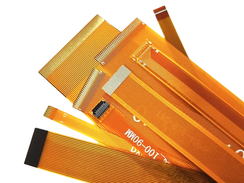
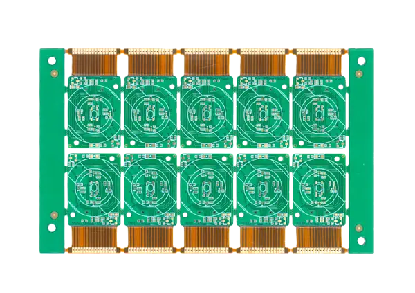
HDI PCBs utilize a variety of advanced technologies to maximize circuit density in space-constrained designs. They have become an indispensable part of everyday products such as smartphones, Bluetooth earphones, smartwatches, and implantable devices, pushing the limits of PCB design and manufacturing.
What makes a HDI PCB?
For many engineers, the term HDI is synonymous with blind and buried vias - the interconnect in High-Density Interconnect. However, HDI boards are characterized by a number of different techniques and features with the shared goal of increasing wiring density:
Microvias
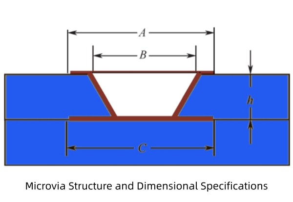
Microvias are vias typically 0.15mm in diameter or less that are laser or chemically drilled. While microvias are technically either blind or buried vias due how they are produced, not all blind/buried vias are microvias. In fact, it is very common in cost-effective buildups to mechanically drill and fill buried vias in the inner core, and reserve laser ablation for the outer blind vias.
Sequential Lamination
Sophisticated HDI stackups with blind and buried vias require multiple, precisely sequenced lamination, drilling, and filling stages. This is one of the major cost and lead time drivers in HDI designs and can be the difference between a hundred to thousands of dollars for a handful of PCBs.
Performance Laminates
Using specialist high-Tg laminates is required to withstand multiple lamination cycles, which also provides significant carry-over benefits for overall board reliability and thermal performance.
Finer traces, pads and smaller component packages
HDI boards are typically characterised by finer trace widths and spacings (PCB Trace Width Calculator), balancing limits of a PCB fabricators capabilities and the traces current carrying requirements. A minimum trace width spacing of 4mil and below is typically considered in the HDI range.
Smaller Component Packages
Real-estate on the outer layers is a highly valuable commodity in HDI designs. HDI designs use the smallest versions of components where possible, with pad sizes less than 0.4mm in size commonplace. Smaller, fine-pitch chips such as BGA, QFN, CSP, etc. packages may necessitate the use of microvias and via-in-pad technology in order to fully breakout all the traces.
HDI PCBs employ a strategic approach combining PCB design and manufacturing techniques and meticulous planning to achieve extreme miniaturization while preserving, and often enhancing, signal integrity and electrical performance. Designers should work with their chosen PCB fab house to formulate the ideal strategy and confirm the most cost-effective buildup early in the design stage.
HDI Buildups - How are HDI PCBs manufactured?
Understanding what is possible and not possible with HDI stackups requires an understanding of PCB lamination structure, drilling capabilities and limits.
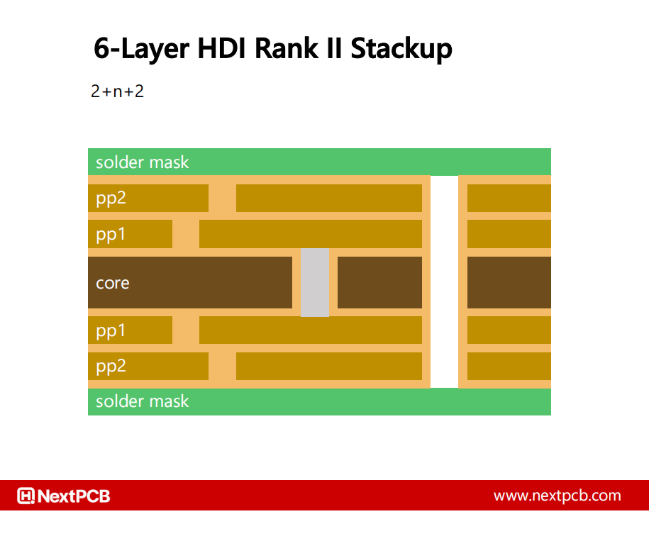
A HDI rank 2 stackup (2+2+2) with two layers of blind microvias on both sides and buried vias in the core
The Small Issue of Aspect Ratio
A key capability in PCB manufacturing is the drill aspect ratio, defined as the ratio of the depth of a hole to its diameter. A manufacturer quoting a maximum aspect ratio of 12:1 can, for example, drill a 0.1mm diameter hole through a 1.2mm thick laminate. A higher ratio, such as 16:1, indicates a more advanced drilling process.
The limitations are twofold:
1) Smaller drill bits are more fragile, require higher spins speeds and are prone to faster wear.
2) Smaller, deeper holes are more difficult to plate uniformly. Specialized equipment is required to force plating fluid to flow into the holes at an adequate rate for a reliable, void-free deposit.
For laser-drilled microvias, aspect ratios are more like 1:1 or 0.75:1 - i.e. laser drilling can only penetrate through a thickness of 0.1mm or 0.075mm - the range of prepreg dielectric layers. In a typical PCB stackup consisting of alternating prepreg and core layers, this complicates HDI buildups and limits the possible interconnections such as eliminating consecutive microvias.
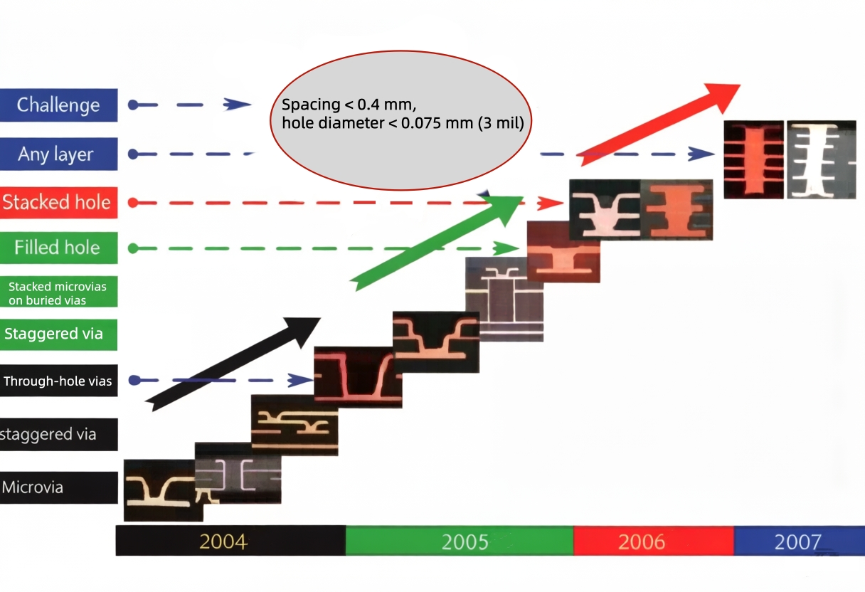
Image source: Internet. Please contact us for removal if there is any infringement.
Plated Via Process:In HDI PCB manufacturing, the plated via process is the dominant approach, accounting for over 95% of the HDI market. It has continued to evolve—from traditional through-hole plating to via filling (copper-filled vias)—significantly increasing design flexibility in HDI boards, as shown in the figure.
HDI Types and Classes
HDI PCBs can be classified in a number of ways. IPC defines construction types that refer to the specific structure of a HDI stackup, for example, 1[C]1 Type 1 is a structure with microvias on both sides of a substrate core, C (as opposed to the copper clad laminate core). HDI classes or ranks are an indication of build-up complexity rather than structure, and generally refer to the number of lamination cycles required to build a specific HDI stackup. E.g. HDI would require one lamination cycle (not including the laminated core), HDI class 2 requires two and so on. In HDI class terms, 1[C]1 type 1 would be a HDI I rank board since it only requires one lamination step in addition to the laminated core.
Similarities diverge when buried vias are introduced. By adding buried vias to the internal core, the above structure becomes a Type 2 HDI board.
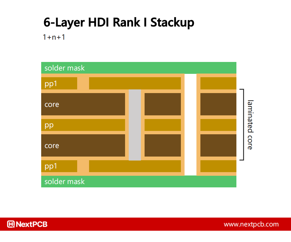
A HDI I rank board with microvias on both sides. The presence of buried vias mean this is a Type 2 HDI structure by IPC definitions.
Takeaway: HDI class is an indication of complexity. HDI Type is a description of a HDI board's structure.
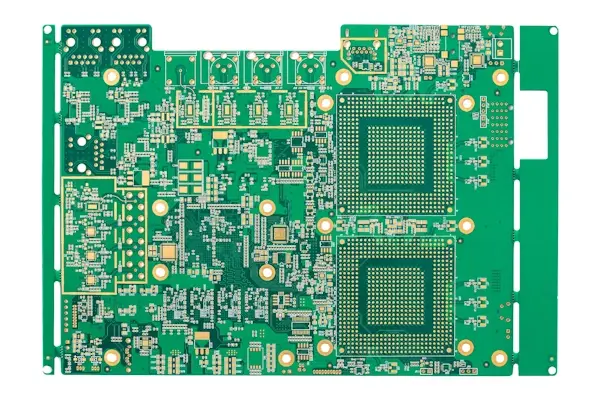
Real-World HDI Application: 14-Layer HDI III PCB
A 14-layer HDI Class III board manufactured for a consumer electronics application, featuring blind vias, small BGA pad size, and controlled impedance on Shengyi substrate.
| Specification |
Detail |
| HDI Class |
HDI III |
| Layer Count |
14 layers |
| Dimensions |
184 × 312mm |
| Board Thickness |
2.0mm |
| Substrate |
Shengyi TG170 |
| Smallest Trace Width |
4 mil |
| Smallest Trace Spacing |
4 mil |
| Min. Hole Diameter |
0.1mm (Blind Via) |
| Min. BGA Pad Size |
0.25mm |
| Impedance Control |
90Ω |
| Surface Finish |
ENIG |
| Solder Mask Color |
Red |
| Application |
Consumer Electronics |
Building HDI Stackups
Each type of via is created and plated separately. For manufacturers, the goal is to accommodate all of the different via configurations requested in as few manufacturing steps as possible. The typical multilayer PCB stackup consisting of alternate stacking of prepregs and cores is highly incompatible with microvia techniques, mainly since microvias cannot be drilled on the thicker cores.
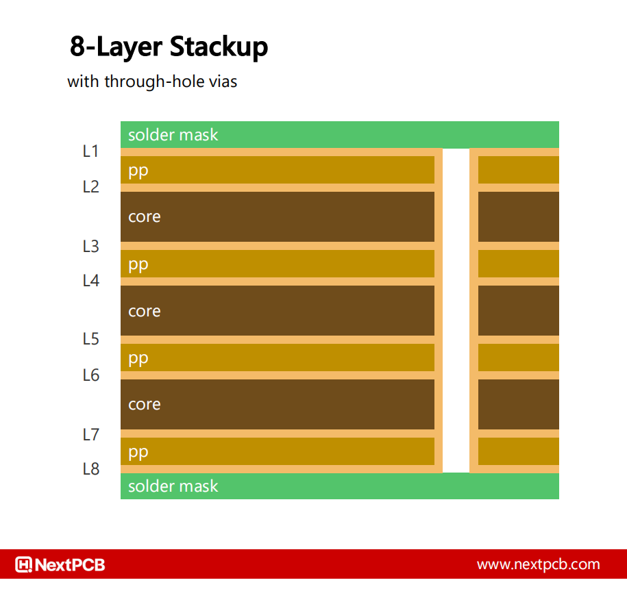
A typical 8 layer stackup
For the novice designer, it may be tempting to connect vias to whatever layers are most convenient for the design, however seemingly simple interconnections can be incompatible or highly inefficient. Even a simple L1 to L2, L1 to L3, L1 to L4 via configuration would require at least 3 lamination stages.
Stacking vias offers maximum design flexibility with the lowest possible footprint, enabling direct connections between non-adjacent layers (L2 to L5 etc.). However, the use of stacked vias is generally not recommended when possible. The process of stacking vias adds a non-trivial increase in manufacturing complexity (and cost), as achieving precision alignment and preserving via integrity is a considerable challenge that can negatively impacts the overall reliability of the via structure.
For example, the most basic 4-layer HDI board has the following stack-up (sometimes referred to an additive stack-up):
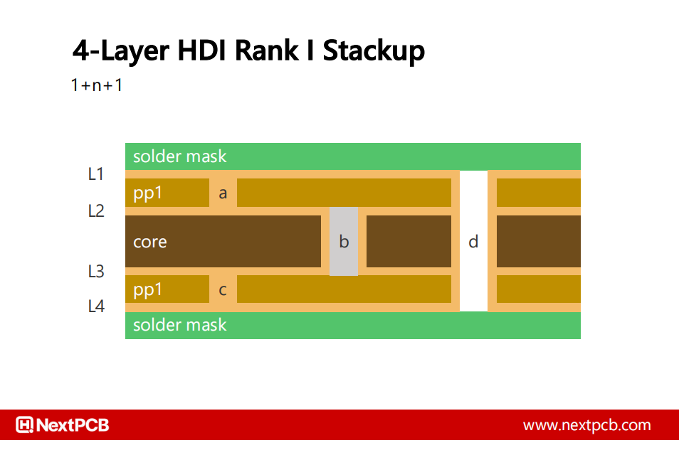
This stack-up allows:
a) L1 - L2 blind vias (laser drilled post lamination)
b) L2 - L3 buried vias (mechanically drilled pre lamination)
c) L3 - L4 blind vias (laser drilled post lamination)
d) Through-hole vias (mechanically drilled post lamination)
Process:
First, the buried vias (b) are drilled on the inner core and filled with non-conductive epoxy, then a layer of prepreg and copper foil are laminated on the top and bottom sides as with a typical multilayer board. A carbon laser then removes material to expose the inner copper. The microvias (a & c) are then cleaned, plated and filled. Standard through-hole vias (d) are then drilled.
If one were to stack vias a) and b) to create a L1 - L3 blind via, the complexity is more akin to HDI class 2 stackup, and would increase the manufacturing cost significantly.
In a quickturn and low-cost setting, HDI technology is difficult to implement consistently due to the need for specialist equipment, precise process control and the lack of pooling opportunities. Therefore, many quickturn manufacturers do not offer HDI manufacture. However, multilayer PCB specialists, NextPCB have conquered the HDI ceiling and offer a selection of cost-effective buildups at a fraction of the cost of traditional alternatives.
High-Density-Interconnect (HDI) PCB Lead Times and Pricing
| Layer Count |
Stackup |
HDI Structure |
Prototype Lead Time |
Prototype Cost |
| 4 layers |
1+2+1 |
1 |
8 days |
From $168 |
| 6 layers |
1+4+1 |
1 |
8 days |
From $223 |
| 8 layers |
1+6+1 |
1 |
8 days |
From $248 |
| 10 layers |
1+8+1 |
1 |
10 days |
From $341 |
| 12 layers |
1+10+1 |
1 |
10 days |
From $406 |
| 14 layers |
1+12+1 |
1 |
10 days |
From $472 |
| 6 layers |
2+2+2 |
2 |
12 days |
From $380 |
| 8 layers |
2+4+2 |
2 |
12 days |
From $394 |
| 10 layers |
2+6+2 |
2 |
14 days |
From $497 |
| 12 layers |
2+8+2 |
2 |
14 days |
From $563 |
| 14 layers |
2+10+2 |
2 |
14 days |
From $628 |
Note: From NextPCB's standard HDI PCB manufacturing service. Prices are in USD and are for reference only. Final pricing vary based on specific board requirements, HDI stackup, and additional services.
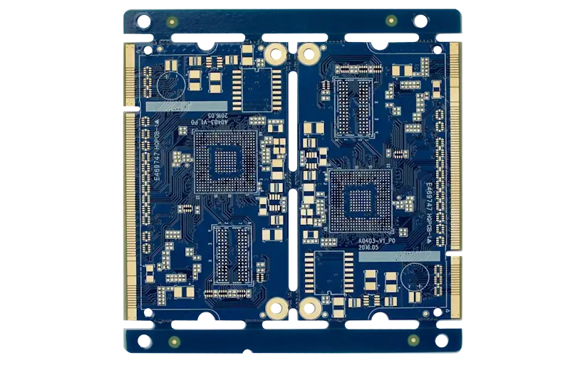
NextPCB HDI PCB Manufacturing Capabilities
NextPCB specilizes in reliable multilayer PCB manufacture including HDI PCBs up to HDI Class 3, and any layer PCBs with the Advanced PCB service for prototype, small batch and mass production requirements. See the table below for a snapshot of our capabilities and services.
| Specification |
Capability |
| HDI Structures |
HDI Class I, II, III, (any layer HDI Advanced PCB) |
| Standard HDI Stack-ups |
1+n+1, 2+n+2, 3+n+3 |
| Materials |
High-TG, High-Speed, High-Frequency laminates and more |
| Vias |
Microvias, blind/buried vias, filled and plated vias/via-in-pad (POVF) |
| Min. Laser Via Diameter |
0.075 - 0.15mm |
| Max. Laser Via Aspect Ratio |
1:1 (0.75:1 recommended) |
| Max. Filled Via Diameter |
0.45mm |
| Blind Via Dimple |
≤10um |
| Min. Trace Width/Spacing |
3.5/3.5 mil (2/2 mil Advanced PCB) |
| Min. Pad Size |
8 mil |
Get an instant quote
Please inquire for more advanced capabilities.
HDI designs rely on stacked microvias to route power between layers — but smaller vias mean tighter current limits. Before finalizing your stackup, check your microvia's current-carrying capacity with our IPC-2221-based calculator.
FAQ
Q: What are the main causes of bottom cracking in 0.1 mm microvias after plating in HDI PCBs?
A: The primary cause is incomplete desmear after laser drilling. Residual resin prevents proper metallurgical bonding between the target pad and the electroless copper layer. Another contributing factor is poor solution exchange in the plating bath, which leads to insufficient copper thickness at the via bottom, making it unable to withstand the significant Z-axis thermal expansion stress during lead-free reflow soldering.
Q: What should I look for when choosing an HDI PCB manufacturer?
A: Key factors include manufacturing certifications (IATF 16949 for automotive, ISO 13485 for medical), demonstrated experience with microvia and sequential lamination processes, IPC Class 2/3 capability, and transparent DFM support before production. Always verify a manufacturer's actual HDI production experience, not just general PCB capacity.
Q: What's the difference between HDI PCB prototyping and mass production manufacturers?
A: Prototype-focused manufacturers prioritize fast turnaround (often 24-48 hours) with smaller batch tolerances, while mass production requires proven process stability, statistical process control (SPC), and consistent yield at scale. NextPCB supports both under the same certified quality system, allowing a seamless transition from prototype to volume production.
Q: Does NextPCB support HDI PCBs for automotive or medical applications?
A: Yes. NextPCB's HDI manufacturing is backed by IATF 16949:2016 certification for automotive-grade traceability and ISO 13485 for medical device quality requirements, alongside RoHS and REACH compliance for global market access.

 NextPCB Capabilities
 PCB Assembly
 Layer Buildup
 SMD-Stencils
 PCB Design-Aid & Layout
 Mechanics
 Surface
 Quality
 Drills & Throughplating
 Factory & Certificate