
 Surface


Zhang

 NextPCB Capabilities
Printed Circuit Boards
NextPCB Capabilities
Printed Circuit Boards
 PCB Assembly
 Layer Buildup
 SMD-Stencils
 PCB Design-Aid & Layout
 Mechanics
 Quality
 Drills & Throughplating
 Factory & Certificate
 PCB Assembly Factory Show
Certificate
PCB Assembly Factory Show
Certificate
Support Team
Feedback:
support@nextpcb.com


In Surface Mount Technology (SMT), solder paste printing is the critical process that determines the final soldering quality. According to industry statistics, over 60% of soldering defects (such as bridging and cold solder joints) originate from improper process control during the printing stage. To ensure high reliability of PCBA, a standardized operating procedure covering material preparation, equipment debugging, environmental control, and quality inspection must be established.
High-quality printing begins with strict control of the physical properties of materials. As a thixotropic fluid, the activity and viscosity of solder paste are directly affected by temperature and mixing time.
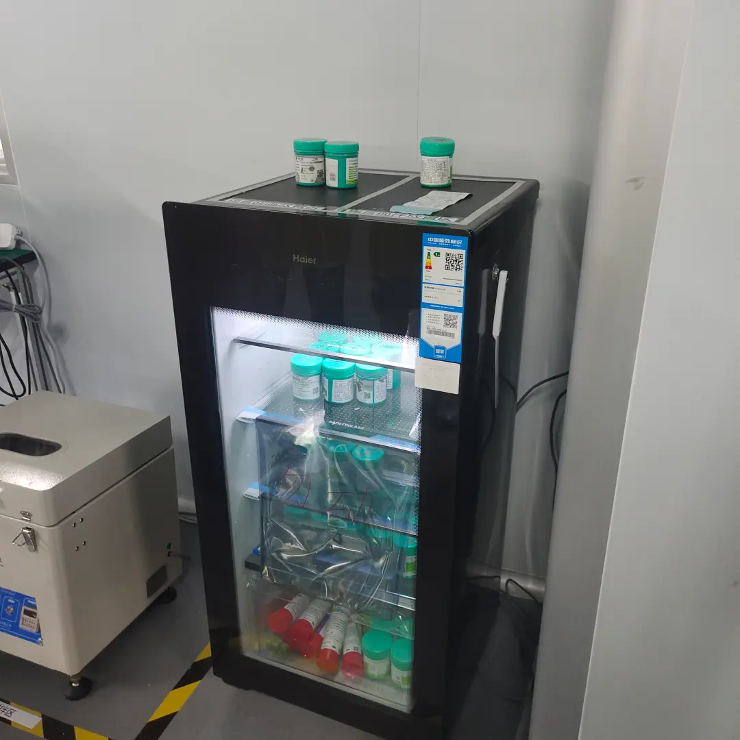
The manufacturing date of the solder paste should not exceed 6 months, and it must be sealed and stored in an environment of 2–10°C. After removal from cold storage, it must undergo at least 2 hours of warming at room temperature to prevent condensation. It is recommended to use up opened solder paste within 24 hours.
Viscosity is a core parameter affecting release performance. Stencil printing typically requires a viscosity range of 900–1400 Pa·s. In applications using Type 3 / Type 4 solder powder with pitches of 0.5mm and below, 900 Pa·s usually demonstrates better release consistency.
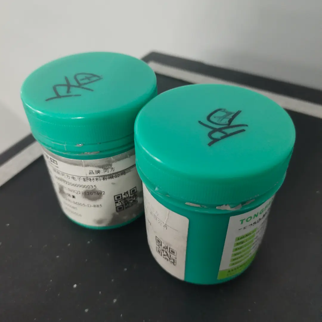
The purpose of mixing is to restore the thixotropy and fluidity of the solder paste.
The moisture absorption status of the substrate directly affects soldering yield. For PCBs with a manufacturing date exceeding 6 months, baking treatment at 125°C for 4 hours is mandatory, typically recommended to be completed the day before production.
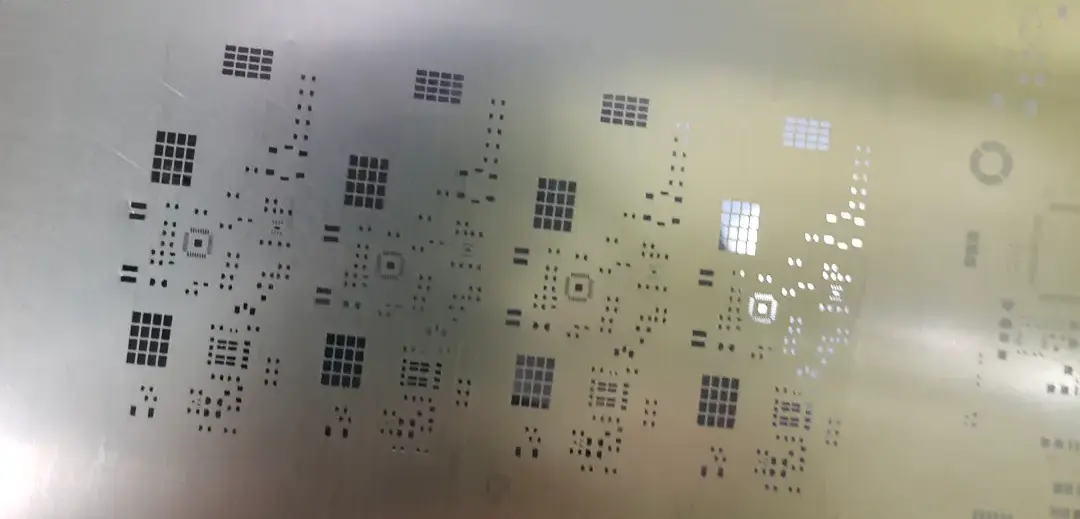
Modern fully automatic printing machines rely on precise parameter settings to ensure repeatability. After equipment initialization, the first step is to input the PCB's length, width, thickness, and Mark point (optical positioning point) data. Mark points effectively correct PCB fabrication errors, requiring clear images, smooth edges, and strong contrast. This practice complies with IPC-7525 basic requirements for printing positioning accuracy and repeatability.
Key process parameters include printing stroke, squeegee pressure, running speed, and separation speed. During the trial run phase, the gap between the PCB and the stencil must be adjusted, typically set to "zero gap" to ensure sealing and prevent solder paste from leaking to the bottom.
Environmental stability during the printing process is crucial for solder paste performance. The production floor should remain windless and clean, with temperature controlled at 23±3°C and relative humidity less than 70%.
The initial amount added should not be excessive; it should ensure a good rolling bead forms in front of the squeegee. Reference addition amounts for different formats are as follows:
During continuous production, operators need to replenish new solder paste in a timely manner to maintain its rolling motion, avoiding uneven squeegee pressure distribution caused by insufficient volume.
The inspection stage is the gatekeeper preventing defective products from flowing into the next process. The choice of inspection method depends on the component density and complexity of the product, and its judgment criteria should be based on IPC-A-610 definitions for solder joint appearance and acceptability, rather than relying solely on subjective experience.
If defects such as bridging, insufficient solder, or deviation are found on QFP pads, the machine should be stopped immediately to analyze the cause. For non-conforming PCBs, the pads must be thoroughly cleaned with anhydrous alcohol before re-printing; direct rework/touch-up is strictly prohibited.
Cleanup work after production tasks directly relates to the equipment status for the next production run. The stencil and squeegee must be thoroughly cleaned. If stencil apertures are blocked, using hard metal needles to forcibly poke them is strictly prohibited to avoid damaging the finish and shape of the aperture walls.
Remaining solder paste should be recovered into a specific container and evaluated for activity before reuse. The printing machine should be returned to the shutdown state, power and air sources cut off, and the daily maintenance log completed according to the equipment maintenance manual.
In the SMT assembly process, statistics show that over 70% of soldering defects originate from the solder paste printing stage. To ensure the reliability of high-precision PCBs, SPI (Solder Paste Inspection) has become an indispensable part of modern manufacturing. Below is an in-depth analysis of the SPI process:
A: Bridging is usually caused by excessive solder volume. For 0.5mm pitch or smaller, you should use an aperture reduction (typically 10-15% smaller than the pad). Stencil thickness should be balanced between 0.10mm and 0.13mm, and electropolished stainless steel is recommended for better paste release.
A: Paste must reach room temperature (2–4 hours) before opening to prevent moisture condensation, which causes "solder balling" or "spattering." Mixing is vital to restore thixotropy (viscosity), ensuring the paste flows through the stencil but holds its shape after printing.
A: The "Type" refers to the sphere size of the solder powder. Type 3 is the industry standard for general PCBAs. However, for 0402, 0201, or micro-BGAs, Type 4 or Type 5 is mandatory to ensure the paste can pass through tiny stencil apertures. If your board has both large and tiny parts, always choose the paste that accommodates the smallest component.
A: Human eyes only see 2D coverage, but SPI measures Volume and Height. Insufficient solder volume (which leads to "dry joints") is nearly impossible to spot manually before reflow. For high-reliability boards, SPI is the most cost-effective way to prevent rework.
A: This is usually a triad of issues:
The stability of the solder paste printing process does not rely on the optimization of a single link but stems from closed-loop control of the entire process, from cold storage to final inspection. NextPCB strictly follows the above process specifications in manufacturing, using the core principles of IPC-7525 and IPC-A-610 as the reference basis for process control and quality judgment. Through refined parameter management and advanced inspection equipment, we ensure that every PCBA achieves the electrical connection performance and mechanical strength expected by the design.
Ready to elevate your SMT yield? Get a High-Precision PCBA Quote from NextPCB Today!

Still, need help? Contact Us: support@nextpcb.com
Need a PCB or PCBA quote? Quote now

