
 Surface


Zhang

 NextPCB Capabilities
Printed Circuit Boards
NextPCB Capabilities
Printed Circuit Boards
 PCB Assembly
 Layer Buildup
 SMD-Stencils
 PCB Design-Aid & Layout
 Mechanics
 Quality
 Drills & Throughplating
 Factory & Certificate
 PCB Assembly Factory Show
Certificate
PCB Assembly Factory Show
Certificate
Support Team
Feedback:
support@nextpcb.com


Table of Contents
Introduction
In today's fast-paced electronics industry, speed and precision are critical factors in transforming an innovative idea into a functional physical device. Engineers spend countless hours perfecting their circuit designs, but until that design is manufactured and tested, it remains just a blueprint. This transformation involves two key stages: PCB fabrication and PCB assembly. Today, we will dive deep into the second, equally vital step: Prototype Assembly.
For many beginners, the word "PCB" often brings to mind a bare, green board etched with intricate copper lines. The manufacturing process for this bare board, often referred to as pcb print or fabrication, is the first step in realizing a design. However, a bare board itself has no function. It's like a building's foundation without a house. To make it "come alive," we must install the brains (ICs), muscles (transistors), and all other electronic components onto it.
This installation process, especially during the small-batch, design-verification stage, is what we call Prototype Assembly.
Before we go further, we must clearly define these two complementary concepts. They represent two key milestones in the journey from blueprint to functional hardware.
A PCB Board Prototype is the physical "skeleton" of your design. It is a bare printed circuit board fabricated according to your design files (e.g., Gerber files).
Core Purpose: Its primary mission is "validation." Before you invest heavily in mass production (which could involve thousands of boards and expensive tooling), you need a low-cost, low-volume way to confirm the design's validity.
What Does It Look Like? This is a board with no electronic components yet installed. You will see the etched copper traces, pads (for soldering components), vias (for connecting different layers), and the solder mask (usually green).
Why "Prototype"? This pcb board prototype is the engineer's testbed. It allows engineers to find and correct design flaws—be it circuit logic errors, traces that are too thin, or component footprint mismatches—at the earliest stage. Rapid iteration and revision are least expensive at this point.
Prototype Assembly is the process of giving "life" to the "skeleton." It refers to the professional service of mounting and soldering all the necessary electronic components (like chips, resistors, capacitors, etc.) onto the pcb board prototype.
Core Purpose: To transform a bare board into a functional "PCBA" (Printed Circuit Board Assembly). Only after assembly can you truly power up the board and test its function.
What Does It Involve? This process strictly follows your Bill of Materials (BOM). It involves highly precise operations, such as:
Why Professional Assembly? Components in modern custom pcb designs are increasingly smaller, with denser pin layouts. Manually soldering prototypes is not only time-consuming but also extremely prone to errors. A professional Prototype Assembly service ensures soldering reliability and consistency, allowing you to focus on design verification, not troubleshooting soldering issues.
In short, the pcb board prototype is the physical carrier of your design, while Prototype Assembly is the essential manufacturing step required to achieve its designed function.
In the custom pcb design flow, prototype assembly is the bridge connecting theory and reality. A design that simulates perfectly in software might fail in the physical world due to component spacing, thermal issues, or slight manufacturing tolerances.
The core value of Prototype Assembly lies in "validation." It proactively answers these key engineering questions:
Through rapid prototype assembly, teams can immediately test firmware, run diagnostics, and validate performance on real hardware, thereby significantly shortening the development cycle.
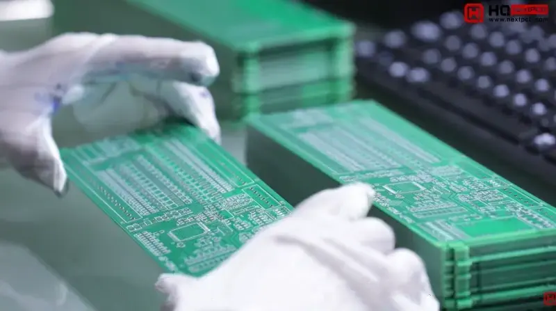
PCB Assembly Process in a State-of-the-Art Factory in China
While DIY (Do-It-Yourself) soldering for a few simple boards is possible, the complexity of modern electronics makes professional assembly a necessity. Today's custom pcb designs often use components as small as 0201 (0.6mm x 0.3mm) or even BGA (Ball Grid Array) packages where the pins are hidden under the chip.
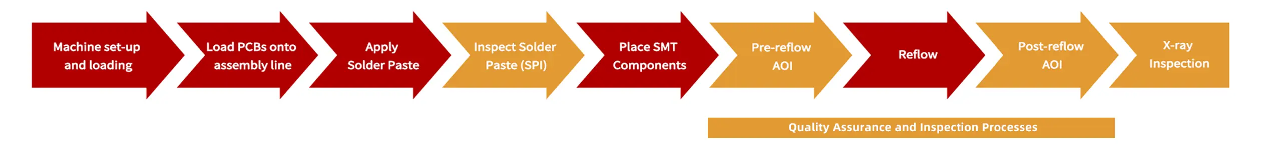
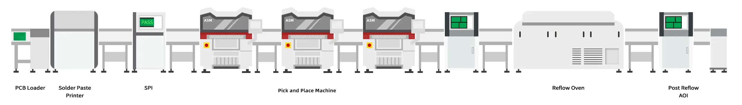
A professional Prototype Assembly service provider (like NextPCB) employs a highly engineered approach to ensure quality and speed:
This is the workhorse of modern assembly.
For components requiring higher mechanical strength, like connectors or large capacitors, THT is still used.
This typically involves manually inserting the components and securing them via wave soldering or selective soldering.

This is the most critical part of Prototype Assembly. Assembly alone is not enough; it must be correct.
Professional services use AOI (Automated Optical Inspection) to scan the board, checking for component shifts, incorrect soldering, or solder bridges.
For invisible solder joints like BGAs, X-ray inspection is used to ensure a good connection.
> Recommend reading: PCB/PCBA Test Methods by Category
For engineers and startups seeking efficiency, the ideal partner is one that offers a "Turnkey" service. This means you only need to upload your design files (Gerbers) and Bill of Materials (BOM), and can then focus on your core design work.
> Want to Build a Killer PCBA BOM? Here's Your Step-by-Step Guide
Using NextPCB as an example, a professional turnkey provider will strictly execute the following process:
The advantage of this integrated method (which we call "Turnkey Service") is obvious. It eliminates the hassle of coordinating multiple suppliers (PCB fab, component distributors, assembly house). Through an optimized process, NextPCB can even offer expedited assembly services as fast as 24 hours. This ensures a seamless transition from bare board fabrication to assembly, which is key to your rapid iteration and market capture.
Prototype Assembly is not just about "soldering parts"; it is a precise engineering process used to validate your custom pcb design and transform your digital blueprint into functional hardware. Whether you are an experienced engineer or a maker just starting, understanding and utilizing professional prototype assembly services is the most reliable way to ensure your pcb board prototype is successful and to accelerate your product's time-to-market.
At NextPCB, we specialize in providing one-stop solutions from PCB prototype fabrication to fast, high-quality assembly. Learn more about our PCB prototype and assembly capabilities and let us help you turn your ideas into reality, faster.

Still, need help? Contact Us: support@nextpcb.com
Need a PCB or PCBA quote? Quote now

