Introduction:
Ball Grid Array (BGA) technology was introduced in the early 1990s as a second-generation surface-mount IC packaging technique by engineers in the United States. The advent of BGA quickly resolved the I/O count bottleneck faced by traditional peripheral-lead packaging techniques like Quad Flat Packages (QFP), making it an indispensable solution in modern electronic devices. Its unique structural design and exceptional electrical performance allow it to support higher I/O densities and superior thermal dissipation, enabling more compact and reliable installations than earlier methods and positioning it as a vital technique in high-density PCB assembly.
The ongoing miniaturization of BGA subsequently led to the emergence of the Chip-Scale Package (CSP) in the late 1990s. CSP, considered a fine-pitch BGA variant, further reduced the package size closer to the chip size, meeting the extreme miniaturization demands of consumer electronics.
This article revisits the fundamental principles, significant advantages, broad application areas, and profound impact of BGA packaging on future technological trends, alongside detailing the precise manufacturing capabilities required when handling cutting-edge BGA design and assembly.

Table of Content:
- 1. What is BGA?
- 2. BGA PCB Layout & Routing Considerations
- 3. BGA Soldering: How It Works
- 4. BGA Rework Process
- 5. The advantages of BGA package
- 6. Application Areas for BGA Packaging
- 7. Impact of BGA Packaging on the Semiconductor Industry
- 8. NEXTPCB BGA Assembly Capabilities & Services
- 9. FAQs
1. What is BGA?
Ball Grid Array (BGA) is a bottom-contact packaging technology widely used in semiconductor chip packaging. Its core feature is the arrangement of chip connection points—known as “bumps”—in a regular grid of solder balls on the bottom of the package, forming a matrix that electrically connects the chip to an external circuit. This packaging method not only enhances heat dissipation but also significantly improves package density and electrical performance.
BGA relies on an interposer or substrate (a small PCB-like layer) that serves as an intermediary between the chip and the host circuit board. The semiconductor chip is attached to the interposer via wire bonding or flip-chip techniques and then typically encapsulated in a protective epoxy. The interposer routes signals from the chip's edges to the solder-ball array, enabling connection to the PCB via reflow soldering, where the solder balls melt to form a reliable electrical connection.
1.1 Structural Anatomy and Function of Ball Grid Array
BGA relies on an interposer or substrate (a small PCB-like layer) that serves as an intermediary between the chip and the host circuit board. The semiconductor chip is attached to the interposer via wire bonding or flip-chip techniques and then typically encapsulated in a protective epoxy. The interposer routes signals from the chip's edges to the solder-ball array, enabling connection to the PCB via reflow soldering, where the solder balls melt to form a reliable electrical connection.
1.2 The Role of Re-Routing in I/O Redistribution
A key technology in BGA substrates is Re-Routing. Re-routing transforms pads originally arranged for wire bonding (typically around the chip’s perimeter) into a regular grid of solder balls on the substrate's underside. This critical step effectively redistributes I/O connections from peripheral wire-bond pads to a structured ball grid array. This transformation is the direct enabler of the high I/O counts required for modern complex ICs, shifting the interconnect paradigm from perimeter-limited leads to an area-distributed array.
1.3 Key Elements of BGA Packaging
1.3.1 Die Attachment / Chip Mounting
The semiconductor die is mounted face-up (or using flip-chip technology) onto the package substrate, typically using solder paste or conductive adhesive, bonding it to the supporting structure.
1.3.2 Solder Ball Array
Solder balls (or "bumps") are arranged in a predetermined grid on the underside of the package (either around the chip’s perimeter or across the bottom) to serve as electrical interconnection points with the external PCB.
1.3.3 Reflow Soldering
The BGA package is placed on the PCB and subjected to a controlled reflow soldering process. During this process, the solder balls melt to form reliable electrical and mechanical bonds. Notably, the surface tension of the molten solder assists in component self-alignment, correcting slight placement inaccuracies.
1.3.4 Encapsulation / Underfill Protection
The packaged chip may be reinforced with plastic encapsulation or underfill materials beneath the solder balls to enhance physical durability, thermal reliability, reinforce joints, and improve thermal management. Underfill is critical for managing the difference in the coefficient of thermal expansion (CTE) between the BGA package and the PCB substrate, preventing solder joint fatigue.
> PCB Thermal Design Basics (1): Substrate Material Selection
> BGA PCB Chip: What Are The Features, Types, and Processes?
1.4 Overview of Common BGA Variants
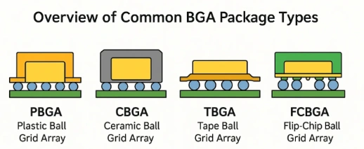
BGA package types lack strict standardization and go by many market-specific names, typically organized by pin count and ball pitch.
- Classic BGA: ~272 pins with 1.27 mm pitch.
- Chip-Scale Package (CSP): ~49 pins with 0.65 mm pitch, considered a fine-pitch BGA, representing further miniaturization.
- Wafer-Level CSP: ~20 pins with 0.4 mm pitch.
- PBGA (Plastic Ball Grid Array): Plastic-encased, known for low cost and suitability for high-volume production.
- CBGA (Ceramic Ball Grid Array): Ceramic-based, offering superior thermal conductivity and electrical performance, but at a higher cost. CBGA is often mandatory for high-power applications like server GPUs that require extremely low thermal resistance, illustrating the causal link between material science and system performance limits.
- TBGA (Tape Ball Grid Array): Constructed using a flexible tape substrate, suitable for high density and performance applications.
- FCBGA (Flip-Chip Ball Grid Array): The chip is flipped and mounted directly onto the substrate, greatly enhancing package density and performance. This variant allows I/O connections to be area-distributed rather than limited to the edges, enabling significantly higher pin counts and improved performance.
> 7 Types of BGA (Ball Grid Array) Packages
2. BGA PCB Layout & Routing Considerations
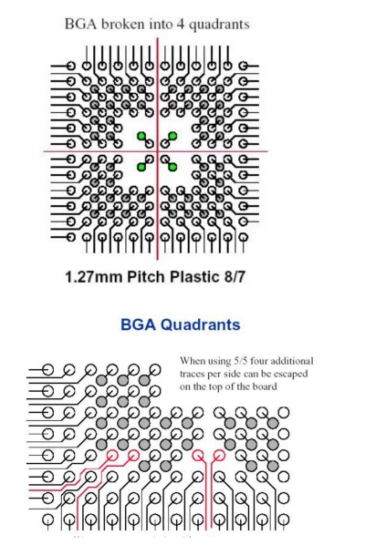
With shrinking BGA pitches and increasing routing density, manufacturers face two main challenges:
- Pad-to-trace clearance constraints: BGA pads often require "windowing," and if your layout does not provide even minimal window clearance, the BGA pad may need to be sacrificed in production.
- Routing via-in-pad: Instead of routing around the pad with dog-bone traces, dense BGA designs rely on placing a via directly within each pad (“via‑in‑pad”) to route signals inward.
- A standard via cannot be used here, because solder may wick into the via during reflow, risking joint integrity.
- The solution: IPC‑4761 Type VII – filled & capped via. These are filled with resin and capped with plating to ensure a smooth, solderable surface.
To fit within BGA pads, these filled & capped vias must be microvias—often laser-drilled. For particularly tight designs, blind microvias may be used. Though technically effective, blind vias carry higher manufacturing costs.
> Recommend Reading: Placement of filter capacitor under BGA
> Recommend Reading: What is a Via in PCB Design and Every Via Type
2.1 General Design and Routing
The continued shrinking of BGA pitches and the increasing routing density present significant challenges for PCB layout. Successful BGA implementation requires designers to strictly adhere to specific design rules related to the BGA's material (most commonly Organic FR-4 or Ceramics).
2.2 Addressing Fine-Pitch BGA Breakout Challenges
In fine-pitch BGAs (especially those with pitches below 1.0 mm), the design challenge revolves around pad-to-trace clearance constraints. These pads often require "windowing"; insufficient minimal window clearance may result in sacrificing the BGA pad during production. Because traditional routing around the pad ("dog-bone" traces) is not feasible, dense BGA designs must rely on placing a via directly within each pad ("via-in-pad") to route signals inward.
2.3 The Importance of Via-in-Pad Technology (IPC-4761 Type VII Standard)
While via-in-pad is necessary for fine-pitch designs, standard vias cannot be used. This is because solder may wick into the via during reflow, risking insufficient solder and compromising joint integrity.
The industry solution is the adoption of IPC-4761 Type VII—the filled and capped via. These vias are filled with resin and then capped with plating to create a smooth, planar, and solderable surface. To fit within BGA pad sizes, these must be microvias (often laser-drilled), or potentially blind microvias for tighter designs, though this incurs higher manufacturing costs. The necessity of IPC-4761 Type VII microvias implies that any product using 1.0 mm or finer pitch BGAs intrinsically requires High-Density Interconnect (HDI) manufacturing capability, directly linking BGA application to increased manufacturing complexity and cost.
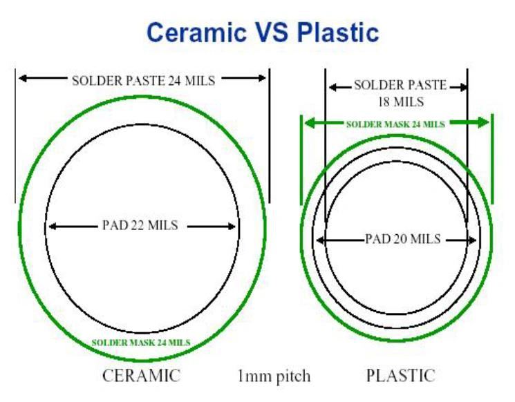
2.4 Comparative Design Rules and Breakout Strategies
Successful BGA implementation requires adherence to specific design rules, often related to the BGA's material (most commonly Organic FR-4 or Ceramics). Design rules vary strictly according to BGA pitch and substrate material.
- Pad Size and Trace/Space Rules (FR-4 Example): The necessary dimensions scale with pitch. For instance:
- 1.27mm Pitch: ~25mil Pad Size, 2X 5/5 Trace/Space.
- 0.8mm Pitch: ~16mil Pad Size, 1X 5/5 Trace/Space.
PAD sizes in FR-4
| Pitch |
Pads Size |
Trace/Space |
Via |
| 1.27mm |
25mil |
2X 5/5 |
25mil |
| 1.0mm |
19mil |
2 X4/4 |
19mil |
| 0.8mm |
16mil |
1X5/5 |
16mil |
PAD sizes in Ceramics
| Pitch |
Pads Size |
Trace/Space |
Via |
| 1.27mm |
28mil |
1top-2bottomX 5/5
|
25mil |
- Breakout Escape: The number of layers needed for signal breakout depends on the pitch. A typical 1.0mm pitch BGA breakout requires 4 layers to escape 6 rows from the top and 6 rows from the bottom (T-6; B-6).
| Pitch |
Breakout Escape rows |
No. of Layers |
| 1.27mm |
T-6; B-6: |
4 |
| 1.0mm |
T-6; B-6: |
4 |
| 0.8mm |
T-4; Any other-6 |
4 |
- Placement Considerations:
- Place the BGA far away from the board edge, leaving at least 200 mils space for rework.
- Do not place components under the BGA.
- Place the fan-out via on a grid.
- Routing Considerations:
- Use a mm grid and dimension for all BGA routes.
- The BGA should be treated as a routing block; avoid routing signals and additional vias underneath the BGA.
- Plug vias from the BGA side.
- Do not pour copper under the BGA top side.
- Connect the power first and keep the 75% rule for power trace.
3. BGA Soldering: How It Works
BGA assembly is characterized by high precision, leveraging physical principles (surface tension) for alignment and requiring specialized inspection methods.
3.1 Solder Paste Application and High-Precision Component Placement
Solder paste is applied to the PCB pads corresponding to the BGA solder balls, typically using a high-precision screen-printing method via a stencil to ensure accuracy and repeatability.
The BGA component is precisely positioned on the PCB using high-precision pick-and-place equipment featuring high-accuracy XY movement and optical alignment systems. Correct initial alignment is critical but not the sole factor in reliability.
> Recommend reading: Common Components on a PCBA and What Matters in Assembly
3.2 Thermal Profiling and Reflow Dynamics
The assembled PCB travels through a reflow oven, following a specific thermal profile tailored to the solder alloy.
- Self-Alignment Mechanism: During the reflow stage, the surface tension of the molten solder pulls the BGA into precise alignment with the PCB pads, thereby correcting slight placement errors.
- Challenge of Hidden Joints: BGA solder joints are hidden beneath the package, making traditional visual inspection (AOI) and electrical testing (ICT) insufficient for detecting latent mechanical issues such as poor wetting, voids, or Head-in-Pillow (HIP) defects.
- The Solution: Automated X-ray Inspection (AXI) is the essential non-destructive method for evaluating BGA solder joints. The X-rays penetrate the package to image the internal solder joints, verifying their quality and reliability.
> Recommend Reading: LGA vs BGA: Which One is Right for You?
3.3 BGA Solder Joint Inspection: Mandatory AXI Requirement
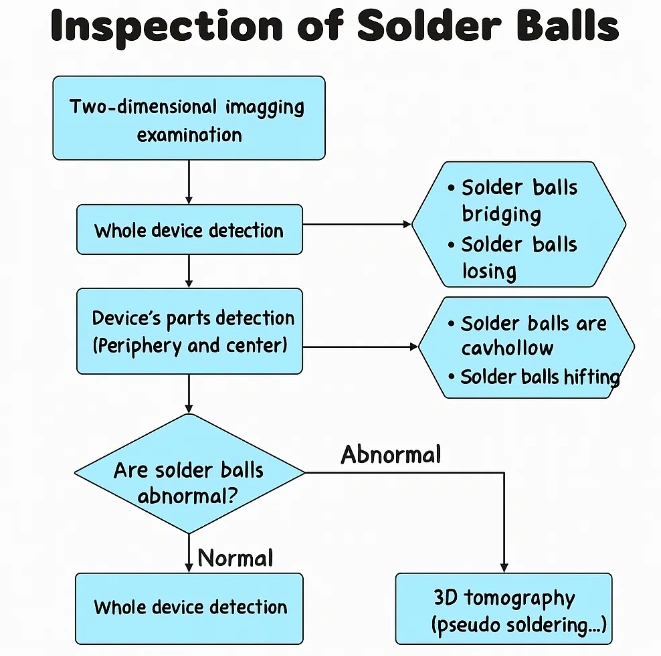
- Challenge of Hidden Joints: BGA solder joints are hidden beneath the package, making traditional visual inspection (AOI) and electrical testing (ICT) insufficient for detecting latent mechanical issues like poor wetting, voids, or “Head-in-Pillow” (HIP) defects.
- Solution: Automated X-ray Inspection (AXI) is the essential non-destructive method for evaluating BGA solder joints. The X-rays penetrate the package to image the internal solder joints, verifying their quality and reliability. For high-density, high-cost assemblies, AXI is not just an inspection, but a mandatory compliance step, serving as the technical guarantor of product quality integrity.
Additional Inspection Techniques
- Dye-and-Pry is a destructive method used when deep failure analysis is needed. In this process, the PCB or assembled component is submerged in a dye, and then mechanically separated; dye penetration at solder interfaces reveals fractures or poor joints.
4. BGA Rework Process
The rework process is initiated when a BGA component is found to be defective, with the goal of safely removing and replacing it without disturbing nearby parts. This process must employ a specialized BGA rework station equipped with controlled heating and airflow.
4.1 Professional BGA Rework Station Necessity
Rework stations use sophisticated area heating (IR and hot air) systems and optical alignment tools to handle the high thermal mass of BGA components and the sensitive surrounding parts.
4.2 Detailed Six-Step Rework Procedure
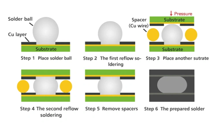
1. Preheat the PCB: The PCB is preheated from below using infrared to approximately 100–120 °C, to minimize thermal shock and board warping. This preheating step is a crucial engineering control for managing the Coefficient of Thermal Expansion (CTE) mismatch between the BGA package, the solder, and the FR-4 substrate. Without this control, differential expansion can lead to catastrophic damage (e.g., delamination or pad lifting).
2. Controlled Heating & Removal: Programmed hot air or IR is used to melt the solder balls (typically 220–240 °C based on the solder type), and then the BGA is gently lifted with a vacuum pickup tool. Precise temperature control is crucial during this step.
3. Site Preparation / Reballing: Residual solder is cleaned using desolder braid or copper coupon methods to ensure a flat, clean pad. If the BGA is being reused, new solder balls are applied via a stencil and the component is reheated to tack them in place (reballing).
4. Component Alignment & Reflow: The BGA is precisely aligned using optical systems. The solder is then reflowed using IR or hot air. It is necessary to follow tight thermal profiles and use minimal airflow to protect adjacent components.
5. Cooling & Lift-off: After reflow, the BGA is gently elevated to avoid disturbing the newly formed joints.
6. Inspection: X-ray inspection (AXI) is conducted to verify joint integrity. This inspection aims to detect defects such as voids, cold solder, misalignment, or “Head-in-Pillow” defects.
4.3 Key Factors for Successful and Reliable BGA Rework
The essential factors required for successful BGA rework include: matching the solder alloy for compatibility ; balancing adhesive strength for positioning; strictly adhering to the thermal profile; using minimal airflow; gently lifting the BGA after reflow; and selecting the correct nozzle size. Skilled technicians and tightly controlled workflows are indispensable. Investment in and adherence to a specialized, controlled rework process significantly enhances the overall yield and reliability of high-value PCBs.
5. The advantages of BGA package
The BGA package is indispensable in modern electronics because it offers systematic technical advantages that support the performance required by today’s miniaturized and high-speed devices.
1. High Density and Maximized Integration: The BGA package provides a solution for producing a small package for an integrated circuit (IC) that has hundreds of pins. This means that fewer components and smaller footprints can be used, which helps to save space on Printed Circuit Boards (PCBs). This highly effective use of PCB space makes it possible to fabricate PCBs for small electronic devices, such as smartphones.
2. Low-Inductance Leads for Optimal High-Speed Electrical Performance: The BGA package requires a shorter electrical conductor, resulting in a lower unwanted (stray) inductance. Since inductance can distort signals in high-speed electronic circuits, the very short distance between the package and the PCB in a BGA results in very low lead inductances, which provides superior electrical performance compared to pinned devices. This shift to area-array packaging is primarily about managing impedance and minimizing signal flight time, making it a technically essential foundation for modern differential pair routing and high-frequency communication protocols (e.g., PCIe, DDR).
3. Better Heat Conduction: The BGA package has lower thermal resistance, which allows the heat produced by the IC to conduct easily. Heat can be dissipated more easily due to the small size of the PCB when using the BGA package. This effective thermal conduction relies on the thermal performance of three sequential layers: die attachment, the BGA substrate (where CBGA excels), and finally, the BGA-to-PCB solder joint.
4. Increase of Manufacturing Yields: The pad in the BGA package is relatively bigger than in other package types, making it easy to solder on a large area. This increases the PCB manufacturing speed and improves manufacturing yields.
5. Fewer Damage Leads: BGA "leads" are composed of solid solder balls, not circuit leads, which makes them less easily damaged or bent during the operation processes.
6. Lower Overall Cost: Although expensive BGA equipment is required for BGA technology, the systematic advantages listed above (reduced material needs, higher yield, and superior thermal/electrical performance) result in a lower overall cost structure.
6. Application Areas for BGA Packaging: Driving Modern Electronics
|
Application Domain
|
Example Uses
|
Key BGA Advantages
|
|
High-Performance Computing
|
Servers, Workstations, High-End GPUs
|
High density, great thermal & electrical performance
|
|
Mobile & Consumer Electronics
|
Smartphones, Tablets, Wearables
|
Compactness, high integration, power efficiency
|
|
Data Center & Networks
|
Switches, Routers, Networking Equipment
|
Scalable density and thermal reliability
|
|
Automotive & Industrial
|
In-Car SoCs, Embedded Storage, Control Systems
|
Rugged reliability, thermal robustness
|
7. Impact of BGA Packaging on the Semiconductor Industry
7.1 Promoting Packaging Technology Advancements
BGA's introduction initiated a transition towards high-density, high-performance packaging methods. It established the technical foundation for more sophisticated variations like FCBGA (Flip-Chip Ball Grid Array) and wafer-level BGA solutions, continually pushing the limits of pin counts and signal performance. In the FCBGA variant, the die is mounted face-down onto a substrate, which allows for area-distributed Input/Output (I/O) connections rather than connections limited to the edges, thereby enabling significantly higher pin counts and improved performance.
7.2 Accelerating System-Level Integration
BGA's high pin density and its superior electrical and thermal performance have spurred innovations in both System-in-Package (SiP) and Multi-Chip Modules (MCM). These integrations facilitate combining multiple chips into a single, compact package, which in turn promotes higher levels of integration and more complex system design capabilities. Since physical limits constrain chip size reduction, SiP/MCM integration, leveraging high-density BGA interconnects, has become the new frontier for achieving miniaturization and performance gains.
7.3 Optimizing Supply Chain Collaboration
The widespread use of BGA packaging necessitates close cooperation across the stages of design, manufacturing, and test (referred to as ATP—Assembly, Test & Packaging). This requirement strengthens a more integrated semiconductor supply chain. As packaging technologies become more advanced and complex, this tight synergy across different domains becomes absolutely critical.
8. NextPCB BGA Assembly Capabilities & Services
NextPCB offers comprehensive services encompassing component sourcing, advanced BGA assembly, and for high-density applications, strictly designed quality assurance protocols.
8.1 Advanced BGA Assembly Specifications
NextPCB is committed to delivering industry-leading BGA assembly capabilities, ensuring the most rigorous design requirements are met.
- Leading Minimum Pitch: NextPCB supports advanced Ball Grid Array (BGA) assembly with a minimum pitch of 0.25mm. This capability addresses the need for the most advanced, smallest electronic devices, significantly surpassing the previously established 0.3mm minimum soldering technology standard.
- High-Density IC Support: Assembly capabilities handle fine-pitch components as small as 0.38mm pitch ICs.
- Minimum Clearance Requirements: The assembly strictly adheres to design rules crucial for maximizing board density, including a minimum distance from the pad to the circuit line of 0.2 mm and a minimum distance between two BGAs of 0.2 mm.
- Assembly Technology Range: Ball-Grid-Array Assembly (BGA) is one of the integrated cutting-edge assembly technologies offered by NextPCB, alongside Surface Mount Technology (SMT) and Through-Hole Technology (THT) solutions.
NextPCB's reliable assembly of 0.25mm pitch BGAs demonstrates technical leadership in process control and equipment investment, capable of supporting clients in fields demanding extreme pitch and reliability, such as high-end mobile and aerospace applications.
NextPCB Advanced BGA Assembly Specifications
|
Capability Item
|
Specification
|
Design Implication
|
|
Supported Minimum BGA Pitch
|
0.25mm
|
Enables assembly of ultra-fine pitch ICs (e.g., advanced processors and memory).
|
|
Fine-Pitch IC Support
|
0.38mm pitch ICs
|
Supports a wide range of high-density package variants.
|
|
Mandatory Quality Assurance
|
X-ray Validation (Mandatory)
|
Guarantees non-destructive inspection of all hidden joints, critical for extreme density.
|
|
Minimum Clearance (Pad-to-Trace)
|
0.2mm
|
Tight routing tolerance maximizes board density.
|
|
Minimum Component Spacing (BGA-to-BGA)
|
0.2mm
|
Optimizes BGA cluster placement efficiency.
|
8.2 Mandatory Quality Assurance Protocols
To ensure the highest reliability for fine-pitch BGAs, the assembly of 0.25mm pitch components requires mandatory X-ray validation (X-ray QA). This critical non-destructive inspection detects internal defects common in ultra-fine pitch assembly, such as voids, bridging, and misalignment. BGA placement – X-RAY checking is a Quality Inspection & Testing Protocol that employs X-ray technology to inspect internal solder joint quality of BGA, QFN, and other packages, ensuring no cold solder joints or bridging.
8.3 Value-Added Services
NextPCB also provides a competitive component purchase service for BGA components. Their expert team can offer professional advice on selecting the best BGA component types to ensure perfect performance for the final product. The company welcomes clients with ideas for PCB prototypes and PCB assembly to make contact.
9. FAQs
1. Can BGA components be reworked or repaired?
Answer: Yes. BGA components can be reworked or repaired using specialized rework stations and techniques such as BGA reballing and hot-air/IR removal. However, this requires precise control, experienced operators, and proper process conditions.
2. What is the difference between lead-free and leaded solder in BGA soldering?
Answer: Lead-free solder (e.g., SAC alloys) is now industry standard due to environmental regulations. It requires higher reflow temperatures compared to traditional leaded solder and may introduce defects such as tin whiskers. Leaded solder, though less environmentally friendly, melts at lower temperatures and is often used in high-reliability contexts.
3. What inspection methods are effective for hidden BGA solder joints?
Answer: Since BGA joints are hidden, X-ray inspection (AXI) is essential for detecting internal defects like voids, cold joints, misalignment, and head-in-pillow issues. AOI and electrical testing may detect surface-level faults but cannot fully assess joint integrity.
4. What is the "head-in-pillow" defect in BGA soldering?
Answer: A head-in-pillow (HIP) defect occurs when the solder ball and solder paste both melt but fail to join—resulting in a visible gap. It's typically caused by oxidation, poor wetting, or thermal distortion during reflow, especially in lead-free processes.
5. What are common challenges in via-in-pad routing for BGA?
Answer: For fine-pitch BGA packages, vias may need to be placed directly within BGA pads (“via-in-pad”) to route from inner balls. Standard vias risk wicking solder and compromising joints. The solution is IPC-4761 Type VII filled & capped microvias, which provide a planar, reliable surface.
6. What are key factors for successful BGA rework?
Answer: Ensure process success by matching solder alloy for compatibility, balancing adhesive strength for positioning, adhering to thermal profile strictly, using minimal airflow, gently lifting the BGA after reflow, and selecting correct nozzle size. Skilled technicians and tightly controlled workflows are essential.
Conclusion
BGA technology remains a cornerstone of the modern electronics roadmap by solving critical challenges related to density, thermal management, and high-speed signal integrity. As devices continue to shrink and performance demands escalate, the complexity of packaging—such as the necessity of IPC-4761 Type VII microvias and mandatory X-ray inspection—will only increase. NextPCB, by offering advanced BGA assembly capabilities down to a minimum pitch of 0.25mm with mandatory X-ray QA , asserts its technical leadership, ensuring customers can confidently deliver the next generation of highly integrated and reliable products.
> Recommend reading: PCB Assembly - The Most Comprehensive Guide | NextPCB
> Recommend reading: Full SMT Assembly Process Guide - SMT Line
About the Author
Arya Li, Project Manager at NextPCB.com
With extensive experience in manufacturing and international client management, Arya has guided factory visits for over 200 overseas clients, providing bilingual (English & Chinese) presentations on production processes, quality control systems, and advanced manufacturing capabilities. Her deep understanding of both the factory side and client requirements allows her to deliver professional, reliable PCB solutions efficiently. Detail-oriented and service-driven, Arya is committed to being a trusted partner for clients and showcasing the strength and expertise of the factory in the global PCB and PCBA market.


 NextPCB Capabilities
 PCB Assembly
 Layer Buildup
 SMD-Stencils
 PCB Design-Aid & Layout
 Mechanics
 Surface
 Quality
 Drills & Throughplating
 Factory & Certificate


