
 Surface


Arya Li, Project Manager at NextPCB.com

 NextPCB Capabilities
Printed Circuit Boards
NextPCB Capabilities
Printed Circuit Boards
 PCB Assembly
 Layer Buildup
 SMD-Stencils
 PCB Design-Aid & Layout
 Mechanics
 Quality
 Drills & Throughplating
 Factory & Certificate
 PCB Assembly Factory Show
Certificate
PCB Assembly Factory Show
Certificate
Support Team
Feedback:
support@nextpcb.com


Table of Contents
Introduction
The era of High-Performance Computing (HPC) demands more from PCBs than ever before. With the rapid evolution of Artificial Intelligence (AI) technology, the need for processing power in data center servers and high-speed switches has reached unprecedented levels. This surge directly results in dramatically increased chip power consumption, making thermal dissipation and Signal Integrity (SI) core challenges that engineers must overcome. This blog post will approach the topic from an engineering and practical perspective, focusing on the selection of high-speed PCB materials, particularly low-loss substrates like the Panasonic Megtron 6/7 series, and how they are key to solving these challenges.
> Visit Advanced PCB Material Collections
HPC workloads, such as AI training and inference, require massive parallel processing and extremely high data transfer rates. This presents two major engineering challenges for the PCBs carrying these systems:
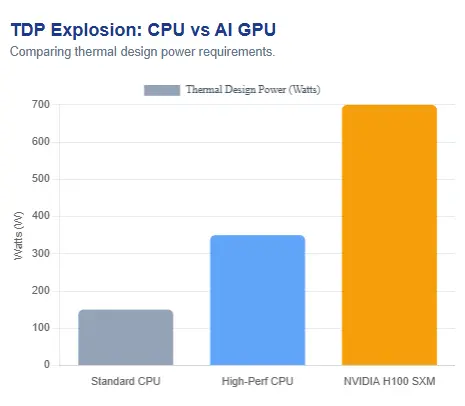
Problem Description: The TDP of advanced GPUs, TPUs, or high-performance CPUs easily exceeds 300W, often reaching 500W or more. For instance, the TDP of an NVIDIA H100 SXM module reaches 700W, pushing rack-level cooling and power distribution to their limits. Traditional cooling solutions struggle to manage localized hot spots, and if heat is not effectively dissipated, it directly impacts chip performance, reliability, and lifespan.
> Fundamentals of PCB Thermal Design | NextPCB
PCB Role: The PCB is not just a carrier for electrical connections; it is also a vital heat dissipation path. The material's thermal conductivity, Coefficient of Thermal Expansion (CTE), and the copper distribution design within the multilayer board are all critical for system-level thermal management.
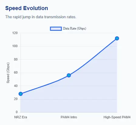
Data rates are transitioning from 28Gbps NRZ/56Gbps PAM4 to 56Gbps PAM4 and even 112Gbps PAM4, with new-generation data center and switch architectures being fully designed around these rate classes. At these frequencies, any minute signal loss (Insertion Loss) or impedance mismatch can cause the Bit Error Rate (BER) to spike, rendering the communication link unusable.
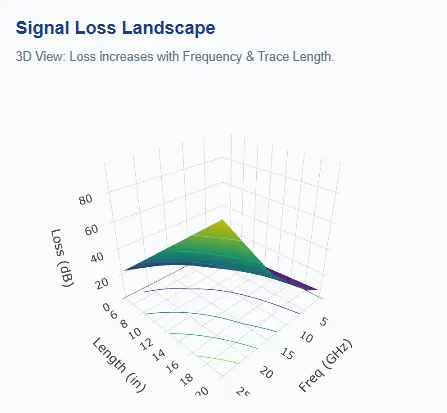
PCB Role: Signals travel through PCB traces. For long-distance high-speed channels like backplanes, both dielectric loss and conductor loss increase significantly at the 25G, 56G, and 112G rate classes. The material's Df and the copper foil roughness are among the key factors determining the channel's insertion loss.
The key to solving this "dual crisis" lies in the heart of the PCB—the laminate material. Engineers are actively seeking high-speed materials that offer both extremely low dielectric loss (Low Loss) and excellent thermal performance.
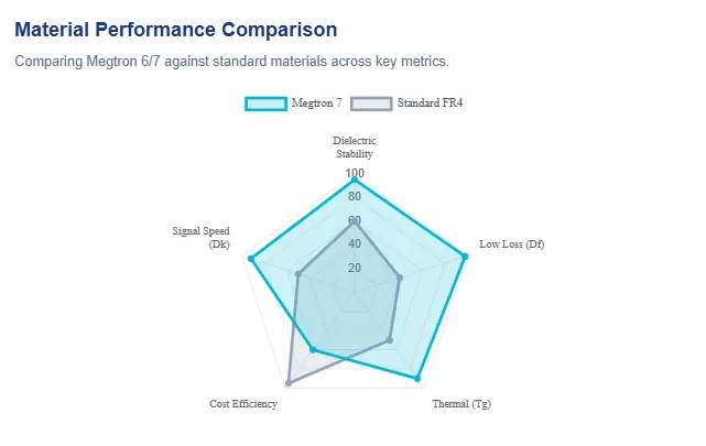
Based on our market insights and engineering search trends, the Panasonic Megtron 6/7 series is a leading choice for current high-speed backplanes and data center server boards. Its core advantages are:
| Parameter | Megtron 6/7 Advantage | Engineering Significance |
|---|---|---|
| Dielectric Constant (Dk) | Low and Stable (approx. 3.3 - 3.7) | 1. Increases signal propagation speed, reducing unit length transmission delay (Tpd).2. Helps maintain stable impedance across a wide frequency band, aiding in crosstalk control through proper trace width/spacing design. |
| Dissipation Factor (Df) | Extremely Low (Typical value approx. 0.0015 – 0.004)Note: Varies slightly with specific grade and frequency | Significantly reduces dielectric loss of high-frequency signals, securing the core metric of the 56G+ signal link budget (Loss Budget). |
| Thermal Performance | High Tg (Glass Transition Temperature) | Improves dimensional stability (low Z-axis expansion) during high-temperature operation and multiple reflow cycles, mitigating barrel failure and delamination risks. |
It is important to note that achieving reliable 112G PAM4 transmission requires more than just low-Df materials. Engineers must simultaneously utilize a suite of system-level complementary designs, including back-drilling, low-roughness copper foil, precise connector selection, and Receiver DSP equalization, to ensure the channel's total loss and jitter are within specification.
Manufacturing requirements for data center server motherboards and high-speed switch backplanes are extremely stringent:
Layer Count Requirement: 20+ layer high-density designs. High layer counts are typically used for complex backplanes or mainboards to separate power/ground planes, signal layers, and provide additional heat dissipation paths.
Low-Loss Substrate: Specified use of Panasonic Megtron 6/7 or equivalent performance grades (e.g., specific models from Rogers, Isola).
Impedance Control: 50 Ω Single-ended, 85 Ω / 100 Ω Differential traces. Precise impedance control is the iron rule for minimizing signal reflection (i.e., optimizing Return Loss).
Under these strict electrical and physical demands, Design for Manufacturability (DFM) becomes the crucial bridge connecting SI simulation with mass production reality. The core of DFM work is translating the required parameters—such as Df, impedance tolerance (e.g., ±5%), and high layer count design—into a stable, achievable stack-up, copper weight distribution, and minimum spacing requirements for the factory. Especially when dealing with complex, high-end processes like back-drilling and embedded copper coins, thorough DFM checks are prerequisite for ensuring product performance and reliability.
High-Speed Switch Backplanes: As the core component connecting all line cards, backplanes are often long, leading to severe signal attenuation. Megtron 7 or equivalent ultra-low-loss materials are typically selected, combined with special stack-up designs (such as using Ultra-Low-Profile copper foil, HVLP) to ensure reliable long-distance high-speed signal transmission.
AI Server Motherboards (OAM/UBB Boards): These carry multiple high-performance AI chips and require complex power/signal distribution networks. High Tg and low Df materials are mandatory, alongside advanced thermal solutions (such as embedded copper coin design or heavy copper technology).
As a specialized high-performance PCB manufacturer, NextPCB understands the manufacturing challenges of the 56G+ era. We are equipped to provide you with:
We possess professional equipment and complete process parameters for handling low-Df materials, ensuring material performance is fully realized during the lamination process.
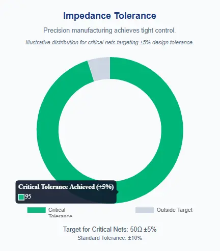
NextPCB offers a ±10% controlled impedance manufacturing tolerance in standard service and supports negotiating tighter targets for critical high-speed links (e.g., aiming for ±5% design requirements). Verification via Impedance Coupon + industrial TDR test systems ensures high consistency between actual test results and SI simulation models.
Experience: Supporting High-Speed Boards up to 32 Layers
We excel at handling high Aspect Ratio designs, Back Drilling processes, and complex mixed-material stack-up structures, meeting the demanding routing needs of high-compute PCBs.
Trustworthiness: Strict Material Supply Chain Management
We ensure all Megtron series materials come from official, genuine manufacturer channels, preventing counterfeits and providing complete CoC (Certificate of Compliance) and test reports.
>> PCB Capabilities - NextPCB >> Turnkey PCB Assembly Services | China PCB Manufacturer - NextPCB
The wave of high-performance computing requires close collaboration between PCB manufacturers and engineers to jointly solve the core conflict between thermal management and signal integrity. Selecting low-loss, high-thermal performance materials like Panasonic Megtron 6/7, combined with precise impedance control and fine-detail, high-layer-count manufacturing, is one of the most practical paths to ensuring reliable signal transmission at 112G and beyond.
NextPCB is committed to being your reliable manufacturing partner in the AI hardware race, transforming the most advanced PCB materials and processes into your successful products.
Are you designing a 32-layer high-speed backplane based on Megtron 7?
We can provide you with stack-up design suggestions and a DFM review report tailored for high-layer count, low-loss materials to help accelerate your project delivery.
Ready for 112G PAM4?
NextPCB combines Megtron 6/7 expertise with advanced processes like back-drilling and
HVLP copper to ensure your AI hardware succeeds.

Still, need help? Contact Us: support@nextpcb.com
Need a PCB or PCBA quote? Quote now

