
 Surface


Julia Wu - Senior Sales Engineer at NextPCB.com

 NextPCB Capabilities
Printed Circuit Boards
NextPCB Capabilities
Printed Circuit Boards
 PCB Assembly
 Layer Buildup
 SMD-Stencils
 PCB Design-Aid & Layout
 Mechanics
 Quality
 Drills & Throughplating
 Factory & Certificate
 PCB Assembly Factory Show
Certificate
PCB Assembly Factory Show
Certificate
Support Team
Feedback:
support@nextpcb.com


The STM32U575 is STMicroelectronics' flagship ultra-low-power microcontroller from the STM32U5 series, built on the ARM® Cortex®-M33 core with TrustZone® security and hardware DSP/FPU acceleration. Available in LQFP48, LQFP64, LQFP80, LQFP144, and UFBGA169 packages, it is designed for the demanding intersection of security-critical IoT applications, industrial wearables, and smart metering systems where power budget, peripheral density, and hardware isolation must coexist on a single die.
This article provides a complete STM32U575 pinout reference across all major package variants, covering GPIO alternate function mappings, power domain pin assignments, analog I/O configuration, and PCB layout considerations specific to the U5 architecture. Engineers migrating from the STM32L4 family should pay particular attention to the expanded power domain structure and the new VDDIO3 supply rail introduced in this series. For the complete HDI routing and DFM checklist applicable to the broader STM32 ecosystem, refer to the STM32 Pinout and Package Guide: High-Speed & HDI Board Layout Best Practices.
The STM32U575 represents a generational leap over the STM32L4 series in three critical dimensions: processing capability (Cortex-M33 vs. Cortex-M4), security architecture (TrustZone® hardware isolation), and analog front-end density (dual 14-bit ADC, 12-bit DAC, OPAMP, and COMP on a single die). Despite these additions, the U5 series maintains the ultra-low-power positioning of its predecessor, achieving run-mode currents below 19 µA/MHz — a benchmark that makes it viable for direct battery operation over multi-year deployment cycles.
| Parameter | STM32U575 | vs. STM32L476 (Reference) |
|---|---|---|
| CPU Core | ARM® Cortex®-M33, 160 MHz | Cortex-M4, 80 MHz |
| Security | TrustZone®, TAMP, AES-256, PKA, RNG, HASH | AES-128, RNG only |
| Flash Memory | Up to 2 MB (dual bank) | Up to 1 MB |
| SRAM | 786 KB (including 64 KB SRAM4 in SRD domain) | 128 KB |
| Operating Voltage (VDD) | 1.71 V – 3.6 V | 1.71 V – 3.6 V |
| Run Mode Current | ≤ 19 µA/MHz (at 3.3 V, Cortex-M33 active) | ≤ 28 µA/MHz |
| Stop 2 Mode Current | ≤ 0.9 µA (with RTC, full SRAM retention) | ≤ 0.4 µA |
| Available Packages | LQFP48, LQFP64, LQFP80, LQFP144, UFBGA169 | LQFP64 to LQFP144, WLCSP81 |
| GPIO Count | Up to 136 (LQFP144 / UFBGA169) | Up to 114 |
| ADC | 2× 14-bit ADC, up to 20 channels each | 3× 12-bit ADC |
| DAC | 2× 12-bit DAC | 2× 12-bit DAC |
| Communication | 4× USART, 2× SPI, 4× I²C, USB OTG FS, FDCAN, OCTOSPI | 3× USART, 3× SPI, 3× I²C, USB FS, CAN |
| Special Features | OCTOSPI (OctoSPI flash), AES accelerator, PKA, UCPD (USB-C PD) | QSPI, AES-128 |
| Temperature Range | -40°C to +85°C (industrial) / +125°C (selected variants) | -40°C to +85°C |
The STM32U575 is pin-to-pin compatible with the STM32U585 (which adds a Neural Processing Unit for on-device ML inference), making it a natural migration path. Engineers planning AI/ML workloads on edge nodes should evaluate the U585 early in the design cycle, as both share identical package footprints and the schematic requires no changes to upgrade.
The STM32U575 is offered in five package configurations targeting different application complexity levels. Package selection directly determines available GPIO count, peripheral accessibility, analog channel density, and whether the OCTOSPI external memory interface is physically routable within your board constraints.
| Package | Pin Count | Body Size | Pitch | Thermal Pad | GPIO | ADC Ch. | Best Use Case |
|---|---|---|---|---|---|---|---|
| LQFP48 | 48 | 7 × 7 mm | 0.5 mm | No | 38 | 12 | Basic IoT sensor nodes, cost-optimized designs |
| LQFP64 | 64 | 10 × 10 mm | 0.5 mm | No | 51 | 16 | Prototyping, wearables with moderate I/O |
| LQFP80 | 80 | 12 × 12 mm | 0.5 mm | No | 67 | 18 | Industrial sensor hubs, OCTOSPI + USB concurrent |
| LQFP144 | 144 | 20 × 20 mm | 0.5 mm | No | 114 | 20 | Full-featured industrial control, motor drive |
| UFBGA169 | 169 | 7 × 7 mm | 0.5 mm | No (exposed VSS balls) | 136 | 20 | HDI space-critical designs, maximum I/O density |
STM32U575 available package options — LQFP48/64/100/144, UFQFPN48, WLCSP90, UFBGA132, and UFBGA169 physical outlines and body dimensions
Unlike the STM32L432 QFN packages, none of the STM32U575 package variants feature a traditional exposed metal thermal pad requiring via-matrix soldering. The UFBGA169 uses exposed VSS balls on the underside periphery for ground connection — these must be connected to the PCB ground plane through their standard BGA pad footprints. The LQFP packages do not expose die substrate and therefore have no thermal pad to manage during assembly. For general thermal pad DFM guidance applicable when using other STM32 QFN variants on the same board, refer to the thermal management section in the STM32 Pinout and Package Guide.
The LQFP64 is the most widely prototyped STM32U575 package, used on the NUCLEO-U575ZI-Q evaluation board (LQFP144) and the B-U585I-IOT02A discovery kit. The 64-pin variant provides a practical balance of I/O count and PCB real estate for wearable and portable industrial designs. Pin 1 is identified by the chamfered corner on the top-left when the package marking is read upright.
| Pin No. | Pin Name | Type | Primary Function | Key Alternate Functions |
|---|---|---|---|---|
| 1 | PC13 | I/O | GPIO / TAMP_IN1 / WKUP2 | RTC_AF1, TAMP_IN1, TAMP_OUT1 |
| 2 | PC14 / OSC32_IN | I/O | GPIO / LSE crystal input | OSC32_IN |
| 3 | PC15 / OSC32_OUT | I/O | GPIO / LSE crystal output | OSC32_OUT |
| 4 | PH0 / OSC_IN | I/O | GPIO / HSE crystal input | OSC_IN |
| 5 | PH1 / OSC_OUT | I/O | GPIO / HSE crystal output | OSC_OUT |
| 6 | NRST | I/O | Reset pin (active low, with internal filter) | — |
| 7 | PC0 | I/O | GPIO / ADC1_IN1 / ADC2_IN1 | LPUART1_RX, I2C3_SCL, LPTIM1_IN1, OCTOSPI1_IO7 |
| 8 | PC1 | I/O | GPIO / ADC1_IN2 / ADC2_IN2 | LPUART1_TX, I2C3_SDA, LPTIM1_OUT, SPI2_MOSI |
| 9 | PC2 | I/O | GPIO / ADC1_IN3 | SPI2_MISO, OCTOSPI1_IO2 |
| 10 | PC3 | I/O | GPIO / ADC1_IN4 | SPI2_MOSI, SAI1_SD_A, OCTOSPI1_IO0 |
| 11 | VSSA | Power | Analog ground | — |
| 12 | VDDA / VREF+ | Power | Analog supply and ADC/DAC reference (shared on LQFP64) | — |
| 13 | PA0 | I/O | GPIO / ADC1_IN5 / WKUP1 | TIM2_CH1, USART2_CTS, COMP1_INP, LPTIM2_ETR |
| 14 | PA1 | I/O | GPIO / ADC1_IN6 | TIM2_CH2, USART2_RTS, I2C1_SMBA, LPTIM2_IN1 |
| 15 | PA2 | I/O | GPIO / ADC1_IN7 / LPUART1_TX | TIM2_CH3, USART2_TX, COMP2_OUT, SAI2_SCK_B |
| 16 | PA3 | I/O | GPIO / ADC1_IN8 / LPUART1_RX | TIM2_CH4, USART2_RX, SAI1_MCLK_A, OCTOSPI1_CLK |
| 17 | PA4 | I/O | GPIO / ADC1_IN9 / DAC1_OUT1 | SPI1_NSS, SPI3_NSS, USART2_CK, LPTIM2_OUT |
| 18 | PA5 | I/O | GPIO / ADC1_IN10 / DAC1_OUT2 | SPI1_SCK, TIM2_CH1_ETR, LPTIM2_ETR |
| 19 | PA6 | I/O | GPIO / ADC1_IN11 / COMP1_OUT | SPI1_MISO, TIM1_BKIN, LPUART1_CTS, TIM3_CH1 |
| 20 | PA7 | I/O | GPIO / ADC1_IN12 / COMP2_INP | SPI1_MOSI, TIM1_CH1N, TIM3_CH2, OCTOSPI1_IO2 |
| 21 | PC4 | I/O | GPIO / ADC1_IN13 / ADC2_IN13 | USART3_TX, OCTOSPI1_IO7 |
| 22 | PC5 | I/O | GPIO / ADC1_IN14 / ADC2_IN14 | USART3_RX, COMP1_INP |
| 23 | PB0 | I/O | GPIO / ADC1_IN15 / ADC2_IN15 | TIM1_CH2N, SPI1_NSS, USART3_CK, OCTOSPI2_IO1 |
| 24 | PB1 | I/O | GPIO / ADC1_IN16 / ADC2_IN16 | TIM1_CH3N, LPUART1_RTS, LPTIM2_IN1, OCTOSPI2_IO0 |
| 25 | PB2 | I/O | GPIO / ADC1_IN17 | LPTIM1_OUT, I2C3_SMBA, SPI3_MOSI, OCTOSPI1_CLK |
| 26 | VSS | Power | Digital ground | — |
| 27 | VDD | Power | Main digital supply (1.71 V–3.6 V) | — |
| 28 | PE7 | I/O | GPIO | TIM1_ETR, UART7_RX, QUADSPI_BK2_IO0, FMC_D4 |
| 29 | PE8 | I/O | GPIO | TIM1_CH1N, UART7_TX, OCTOSPI1_IO6, FMC_D5 |
| 30 | PE9 | I/O | GPIO | TIM1_CH1, UART7_RTS, OCTOSPI1_IO4, FMC_D6 |
| 31 | PE10 | I/O | GPIO | TIM1_CH2N, UART7_CTS, OCTOSPI1_IO5, FMC_D7 |
| 32 | PE11 | I/O | GPIO | TIM1_CH2, SPI2_NSS, OCTOSPI2_NCS, FMC_D8 |
| 33 | PE12 | I/O | GPIO | TIM1_CH3N, SPI2_SCK, OCTOSPI2_CLK, FMC_D9 |
| 34 | PE13 | I/O | GPIO | TIM1_CH3, SPI2_MISO, OCTOSPI2_IO0, FMC_D10 |
| 35 | PE14 | I/O | GPIO | TIM1_CH4, SPI2_MOSI, OCTOSPI2_IO1, FMC_D11 |
| 36 | PE15 | I/O | GPIO | TIM1_BKIN2, USART3_RX, FMC_D12, DCMI_D3 |
| 37 | PB10 | I/O | GPIO | I2C2_SCL, SPI2_SCK, USART3_TX, TIM2_CH3 |
| 38 | PB11 | I/O | GPIO | I2C2_SDA, USART3_RX, TIM2_CH4, LPUART1_TX |
| 39 | VDDIO2 | Power | Dedicated I/O supply for Port G (1.08 V–3.6 V) | — |
| 40 | PB12 | I/O | GPIO | SPI2_NSS, I2C2_SMBA, USART3_CK, TIM1_BKIN |
| 41 | PB13 | I/O | GPIO | SPI2_SCK, TIM1_CH1N, LPUART1_CTS, I2C2_SCL |
| 42 | PB14 | I/O | GPIO | SPI2_MISO, TIM1_CH2N, USART3_RTS, I2C2_SDA |
| 43 | PB15 | I/O | GPIO | SPI2_MOSI, TIM1_CH3N, RTC_REFIN, TIM15_CH1N |
| 44 | VDDUSB | Power | USB transceiver supply (3.0 V–3.6 V) | — |
| 45 | PA8 | I/O | GPIO / USB_SOF / MCO | TIM1_CH1, I2C3_SCL, USART1_CK, SAI1_SCK_A |
| 46 | PA9 | I/O | GPIO / USB_VBUS | TIM1_CH2, USART1_TX, I2C3_SDA, SAI1_FS_A |
| 47 | PA10 | I/O | GPIO / USB_ID | TIM1_CH3, USART1_RX, I2C3_SMBA, SAI1_SD_A |
| 48 | PA11 | I/O | GPIO / USB_DM | TIM1_CH4, USART1_CTS, CAN1_RX, UCPD1_CC1 |
| 49 | PA12 | I/O | GPIO / USB_DP | TIM1_ETR, USART1_RTS, CAN1_TX, UCPD1_CC2 |
| 50 | PA13 / JTMS-SWDIO | I/O | SWD data / GPIO | IR_OUT, USB_NOE |
| 51 | PA14 / JTCK-SWCLK | I/O | SWD clock / GPIO | LPTIM1_OUT |
| 52 | PA15 / JTDI | I/O | GPIO | SPI1_NSS, SPI3_NSS, TIM2_CH1_ETR, USART2_RX |
| 53 | PC10 | I/O | GPIO | SPI3_SCK, USART3_TX, UART4_TX, SDMMC1_D2 |
| 54 | PC11 | I/O | GPIO | SPI3_MISO, USART3_RX, UART4_RX, SDMMC1_D3 |
| 55 | PC12 | I/O | GPIO | SPI3_MOSI, USART3_CK, UART5_TX, SDMMC1_CK |
| 56 | PD2 | I/O | GPIO | UART5_RX, TIM3_ETR, SDMMC1_CMD, OCTOSPI1_NCS |
| 57 | PB3 / JTDO-TRACESWO | I/O | GPIO / SWO trace | SPI1_SCK, SPI3_SCK, TIM2_CH2, USART1_RTS |
| 58 | PB4 / NJTRST | I/O | GPIO | SPI1_MISO, SPI3_MISO, TIM3_CH1, USART1_CTS |
| 59 | PB5 | I/O | GPIO | SPI1_MOSI, SPI3_MOSI, TIM3_CH2, I2C1_SMBA |
| 60 | PB6 | I/O | GPIO | USART1_TX, I2C1_SCL, TIM4_CH1, LPTIM1_ETR |
| 61 | PB7 | I/O | GPIO | USART1_RX, I2C1_SDA, TIM4_CH2, LPTIM1_IN2 |
| 62 | BOOT0 | Input | Boot mode selection (hardware pin, unlike STM32L432) | — |
| 63 | PB8 | I/O | GPIO | I2C1_SCL, TIM4_CH3, SDMMC1_D4, FDCAN1_RX |
| 64 | PB9 | I/O | GPIO | I2C1_SDA, TIM4_CH4, SDMMC1_D5, FDCAN1_TX |
Note that Pin 62 on the STM32U575 LQFP64 is a dedicated hardware BOOT0 pin — unlike the STM32L432 where boot mode is controlled via option bytes. On the U575, BOOT0 must be pulled low (to VSS) through a 10 kΩ resistor for normal Flash boot operation. Add a test point or zero-ohm jumper to allow pulling BOOT0 high for DFU recovery without board modification.
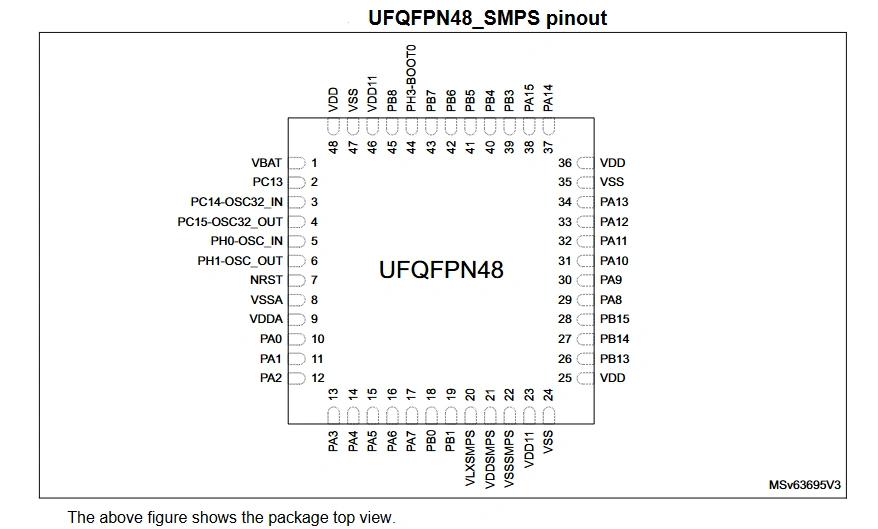
The UFQFPN48 package is the most compact STM32U575 option at 7 × 7 mm with 0.5 mm pitch. The SMPS variant introduces three dedicated power management pins — VLXSMPS (switching node), VDDSMPS (SMPS output), and VSSSSMPS (SMPS ground) — replacing the standard VDD/VSS pins at those positions. These pins must be connected to the external SMPS inductor and filter network; they cannot be left floating or tied to the main VDD plane.
STM32U575 UFQFPN48 SMPS variant pinout — top view showing VLXSMPS, VDDSMPS, VSSSSMPS dedicated power management pins replacing standard supply positions

Note that PH3-BOOT0 appears as a labeled pin (Pin 44) on this package variant, confirming that BOOT0 is a hardware pin on all STM32U575 packages — not option-byte controlled as on STM32L432. Pull Pin 44 to VSS via a 10 kΩ resistor for normal Flash boot operation.
The LQFP144 expands the accessible peripheral set to its maximum, exposing the full OCTOSPI1 and OCTOSPI2 interfaces, SDMMC1 and SDMMC2 buses, FDCAN, and the complete 20-channel dual ADC configuration. It is the reference package for the NUCLEO-U575ZI-Q evaluation board and is the preferred choice for industrial gateway and data-acquisition system designs.
The LQFP144 distributes 36 pins per side at 0.5 mm pitch on a 20 × 20 mm body. The pin table below covers the power, control, and high-speed interface pins most critical for schematic design. For the complete 144-pin assignment, always cross-reference the official STM32U575 datasheet before committing to layout.
| Pin No. | Pin Name | Type | Primary Function | Key Alternate Functions |
|---|---|---|---|---|
| 1 | PE2 | I/O | GPIO | TRACECLK, SPI1_SCK, SAI1_MCLK_A, OCTOSPI1_IO2 |
| 2 | PE3 | I/O | GPIO | TRACED0, SAI1_SD_B, OCTOSPI1_CLK |
| 3 | PE4 | I/O | GPIO | TRACED1, SPI1_NSS, SAI1_FS_A, DCMI_D4 |
| 4 | PE5 | I/O | GPIO | TRACED2, SPI1_MISO, SAI1_SCK_A, TIM15_CH1 |
| 5 | PE6 | I/O | GPIO | TRACED3, SPI1_MOSI, SAI1_SD_A, TIM15_CH2 |
| 6 | PC13 | I/O | GPIO / TAMP_IN1 | RTC_AF1, TAMP_OUT1, WKUP2 |
| 7 | PC14 / OSC32_IN | I/O | GPIO / LSE in | OSC32_IN |
| 8 | PC15 / OSC32_OUT | I/O | GPIO / LSE out | OSC32_OUT |
| 9 | PF0 | I/O | GPIO | I2C2_SDA, OCTOSPI2_IO0, FMC_A0 |
| 10 | PF1 | I/O | GPIO | I2C2_SCL, OCTOSPI2_IO1, FMC_A1 |
| 11 | PF2 | I/O | GPIO | I2C2_SMBA, OCTOSPI2_IO2, FMC_A2 |
| 12 | PF3 | I/O | GPIO | ADC1_IN18, OCTOSPI2_IO3, FMC_A3 |
| 13 | PF4 | I/O | GPIO | ADC1_IN19, OCTOSPI2_IO4, FMC_A4 |
| 14 | PF5 | I/O | GPIO | ADC2_IN19 / ADC2_IN20, OCTOSPI2_IO5, FMC_A5 |
| 15 | PH0 / OSC_IN | I/O | GPIO / HSE crystal in | OSC_IN |
| 16 | PH1 / OSC_OUT | I/O | GPIO / HSE crystal out | OSC_OUT |
| 17 | NRST | I/O | Reset (active low, filtered) | — |
| 18 | PC0 | I/O | GPIO / ADC1_IN1 / ADC2_IN1 | LPUART1_RX, I2C3_SCL, LPTIM1_IN1, OCTOSPI1_IO7 |
| 19 | PC1 | I/O | GPIO / ADC1_IN2 / ADC2_IN2 | LPUART1_TX, I2C3_SDA, SPI2_MOSI, LPTIM1_OUT |
| 20 | PC2 | I/O | GPIO / ADC1_IN3 | SPI2_MISO, OCTOSPI1_IO2, I2C3_SCL |
| 21 | PC3 | I/O | GPIO / ADC1_IN4 | SPI2_MOSI, SAI1_SD_A, OCTOSPI1_IO0 |
| 22 | VSSA | Power | Analog ground | — |
| 23 | VREF+ | Power | Dedicated ADC/DAC external reference input | — |
| 24 | VDDA | Power | Analog supply for ADC, DAC, COMP, OPAMP | — |
| 25–36 | PA0–PA11 | I/O | GPIO / ADC1_IN5–16 / DAC / COMP / WKUP / USB | See LQFP64 table for PA0–PA11 alternate functions; identical on LQFP144 |
| 50 | VSS | Power | Digital ground (first instance) | — |
| 51 | VDD | Power | Main digital supply (first instance) | — |
| 57 | VDDIO2 | Power | Port G I/O supply (1.08 V–3.6 V), independent voltage domain | — |
| 73 | VDDUSB | Power | USB PHY supply (3.0 V–3.6 V) | — |
| 95 | VSS | Power | Digital ground (second instance) | — |
| 96 | VDD | Power | Main digital supply (second instance) | — |
| 108 | PG2 | I/O | GPIO (VDDIO2 domain) | TIM8_ETR, SPI1_SCK, OCTOSPI2_IO6, FMC_A12 |
| 109 | PG3 | I/O | GPIO (VDDIO2 domain) | OCTOSPI2_IO7, FMC_A13 |
| 131 | BOOT0 | Input | Hardware boot mode pin — pull to VSS for Flash boot | — |
| 143 | VSS | Power | Digital ground (third instance) | — |
| 144 | VDD | Power | Main digital supply (third instance) | — |
The LQFP144 separates VREF+ and VDDA onto independent pins (Pins 23 and 24 respectively), unlike the LQFP64 where they share a single pad. This separation is essential for precision ADC designs: VDDA supplies the analog peripheral bias current while VREF+ independently defines the ADC conversion reference voltage. Driving VREF+ from a dedicated precision voltage reference (e.g., REF3033 or similar) eliminates the noise coupling path from analog bias current transients into the conversion reference — a common source of ADC non-linearity in mixed-signal designs.
The UFBGA169 packs 169 balls in a 13×13 grid array on a 7 × 7 mm body at 0.5 mm ball pitch. It provides the highest available GPIO count (136 pins) and is the only STM32U575 package that can simultaneously route both OCTOSPI interfaces alongside SDMMC1, FDCAN, and USB without GPIO multiplexing conflicts. This makes it the preferred package for IoT gateway and industrial data concentrator designs where peripheral density must be maximized within strict area constraints.
| Ball | Pin Name | Type | Notes |
|---|---|---|---|
| A1 | PE2 | I/O | TRACECLK / SPI1_SCK / OCTOSPI1_IO2 |
| A2 | PE4 | I/O | SPI1_NSS / SAI1_FS_A / DCMI_D4 |
| A3 | PE6 | I/O | SPI1_MOSI / SAI1_SD_A / TIM15_CH2 |
| A4 | PF2 | I/O | I2C2_SMBA / OCTOSPI2_IO2 / FMC_A2 |
| A5 | PF4 | I/O | ADC1_IN19 / OCTOSPI2_IO4 / FMC_A4 |
| A6 | PF6 | I/O | OCTOSPI2_IO6 / FMC_NIORD / TIM5_CH1 |
| A7 | PF8 | I/O | OCTOSPI2_IO0 / SAI1_SCK_B / TIM5_CH3 |
| A8 | PF10 | I/O | ADC2_IN6 / OCTOSPI2_CLK / DCMI_D11 |
| A9 | PA2 | I/O | ADC1_IN7 / LPUART1_TX / TIM2_CH3 |
| A10 | PA5 | I/O | ADC1_IN10 / DAC1_OUT2 / SPI1_SCK |
| A11 | PA8 | I/O | USB_SOF / MCO / TIM1_CH1 / I2C3_SCL |
| A12 | PA11 | I/O | USB_DM / UCPD1_CC1 / CAN1_RX |
| A13 | PA14 / JTCK-SWCLK | I/O | SWD clock — reserve for debug |
| B1 | PE3 | I/O | TRACED0 / SAI1_SD_B / OCTOSPI1_CLK |
| B2 | PE5 | I/O | TRACED2 / SPI1_MISO / TIM15_CH1 |
| B3 | PF0 | I/O | I2C2_SDA / OCTOSPI2_IO0 / FMC_A0 |
| B4 | PF3 | I/O | ADC1_IN18 / OCTOSPI2_IO3 / FMC_A3 |
| B5 | PF5 | I/O | ADC2_IN19 / OCTOSPI2_IO5 / FMC_A5 |
| B6 | PF7 | I/O | OCTOSPI2_IO7 / SAI1_MCLK_B / TIM5_CH2 |
| B7 | PF9 | I/O | OCTOSPI2_IO1 / SAI1_FS_B / TIM5_CH4 |
| B8 | VSSA | Power | Analog ground |
| B9 | VDDA | Power | Analog supply — connect 1 nF + 1 µF to VSSA |
| B10 | PA4 | I/O | ADC1_IN9 / DAC1_OUT1 / SPI1_NSS |
| B11 | PA9 | I/O | USB_VBUS / TIM1_CH2 / USART1_TX / I2C3_SDA |
| B12 | PA12 | I/O | USB_DP / UCPD1_CC2 / CAN1_TX |
| B13 | PA13 / JTMS-SWDIO | I/O | SWD data — reserve for debug |
| C1–C13 through M1–M13 | Port B, C, D, E, F, G, H, I signals + VSS/VDD/VDDIO2/VDDUSB/BOOT0/NRST | Mixed | Full ball map in STM32U575 datasheet Table 26. Inner balls (D4–L10) carry Port G (VDDIO2 domain), FMC bus, OCTOSPI data lanes, and multiple VSS/VDD islands. |
| G7 | VSS | Power | Central ground ball — part of inner VSS island |
| H7 | VDD | Power | Central supply ball |
| G8 | VDDIO2 | Power | Port G domain supply — may differ from VDD |
| H8 | VDDUSB | Power | USB PHY supply — must be 3.0 V minimum |
BGA routing for the UFBGA169 requires a minimum of 4 PCB layers to successfully fan out all balls: one signal layer above the BGA, one ground reference layer, one power layer, and one additional signal layer for escape routing. At 0.5 mm pitch, via-in-pad (VIPPO) processing is required for inner ball rows where there is insufficient space for conventional dogbone via fanout. Specify this explicitly in your PCB fabrication requirements — VIPPO requires epoxy fill, copper cap plating, and surface planarization and is not included in standard manufacturing.
The STM32U575 uses the same AF0–AF15 alternate function numbering convention as all STM32 devices, but the peripheral-to-AF mapping has been updated relative to the STM32L4 family to accommodate new U5-series peripherals including OCTOSPI, UCPD, FDCAN, and the expanded timer set. Do not assume STM32L476 or STM32L432 alternate function assignments carry forward to the U575 without verification.
| AF Code | Peripheral Group | Key Functions |
|---|---|---|
| AF0 | System | MCO, SWJ (SWDIO, SWCLK, SWO, JTDI), RTC_REFIN, TRACED0–3, TRACECLK, EVENTOUT |
| AF1 | TIM1 / TIM2 / TIM5 / TIM8 | TIM1_CH1–CH4, TIM1_BKIN/BKIN2, TIM2_CH1–CH4, TIM5_CH1–CH4, TIM8_CH1–CH4 |
| AF2 | TIM1 / TIM2 / TIM3 / TIM4 / TIM5 / LPTIM3 | TIM1_CH1N–CH3N, TIM2_ETR, TIM3_CH1–CH4, TIM4_CH1–CH4, LPTIM3_OUT |
| AF3 | USB / OCTOSPI1 / TIM8 / SPI2 | USB_NOE, OCTOSPI1_IO0–IO7 (partial), TIM8_CH1N–CH3N, SPI2_NSS |
| AF4 | I²C 1 / I²C 2 / I²C 3 / I²C 4 | I2C1_SCL/SDA/SMBA, I2C2_SCL/SDA/SMBA, I2C3_SCL/SDA/SMBA, I2C4_SCL/SDA |
| AF5 | SPI 1 / SPI 2 / SPI 3 | SPI1_SCK/MISO/MOSI/NSS, SPI2_SCK/MISO/MOSI/NSS, SPI3_SCK/MISO/MOSI/NSS |
| AF6 | SPI 3 / I2C 3 / OCTOSPI1 | SPI3_SCK/MISO/MOSI, I2C3_SCL/SDA, OCTOSPI1_NCS/CLK/IO0–IO7 |
| AF7 | USART 1 / USART 2 / USART 3 | USART1_TX/RX/CK/CTS/RTS, USART2_TX/RX/CK/CTS/RTS, USART3_TX/RX/CK/CTS/RTS |
| AF8 | UART 4 / UART 5 / LPUART 1 / SDMMC 1 | UART4_TX/RX, UART5_TX/RX, LPUART1_TX/RX/CTS/RTS, SDMMC1_D0–D3/CK/CMD |
| AF9 | FDCAN 1 / TIM15 / LPTIM 2 / OCTOSPI2 | FDCAN1_TX/RX, TIM15_CH1/CH2/BKIN, LPTIM2_ETR/IN1/IN2/OUT, OCTOSPI2_NCS |
| AF10 | USB / OCTOSPI 1 / OCTOSPI 2 / DCMI / SDMMC 2 | USB_CRS_SYNC, OCTOSPI1_CLK/NCS/IO0–IO7, OCTOSPI2_CLK/IO0–IO7, DCMI_D0–D11, SDMMC2_CK/CMD/D0–D7 |
| AF11 | UCPD 1 / I2C 4 / LPTIM 1 | UCPD1_CC1/CC2/FRSTX, I2C4_SCL/SDA, LPTIM1_ETR/IN1/IN2/OUT |
| AF12 | FMC / SDMMC 1 / COMP | FMC_D0–D15/A0–A25/NOE/NWE/NCS/CLK, SDMMC1_D4–D7, COMP1_OUT, COMP2_OUT |
| AF13 | SAI 1 / SAI 2 / DCMI | SAI1_SCK_A/FS_A/SD_A/MCLK_A, SAI1_SD_B/FS_B, SAI2_SCK_B/FS_B/SD_B/MCLK_B, DCMI_D0–D7 |
| AF14 | TIM 2 / LPTIM 2 / TIM 15 / TIM 16 / TIM 17 | TIM2_CH1–CH4, LPTIM2_ETR/OUT, TIM15_CH1N, TIM16_CH1/BKIN, TIM17_CH1/BKIN |
| AF15 | Event Out | EVENTOUT (software-triggered output, any GPIO) |
A critical difference from STM32L4: the OCTOSPI interfaces consume AF3, AF6, AF10 across a large number of Port A, B, C, E, F, and G pins. If your design uses OCTOSPI external flash or PSRAM, perform the pin assignment in STM32CubeMX before placing any other peripheral — OCTOSPI has the most constrained routing and consumes the most AF slots of any peripheral in the U575 portfolio.
The STM32U575 introduces a three-domain power architecture that is more complex than the STM32L4 series. Understanding each domain's voltage constraints and sequencing requirements is mandatory before finalizing the power delivery network schematic.
| Domain | Supply Pin(s) | Voltage Range | Powered Peripherals | Decoupling Requirement |
|---|---|---|---|---|
| Main digital | VDD / VSS | 1.71 V – 3.6 V | Core, flash, most GPIO, timers, comms peripherals | 100 nF + 4.7 µF per VDD pin; multiple VDD pins on LQFP144 — decouple each independently |
| Analog | VDDA / VSSA | 1.71 V – 3.6 V (≥ VDD) | ADC1, ADC2, DAC1, COMP1, COMP2, OPAMP1, VREFINT, VREFBUF | 1 nF + 1 µF to VSSA; supply via ferrite bead from VDD rail |
| ADC/DAC reference | VREF+ / VSSA | 1.8 V – VDDA | ADC conversion reference only (independent of VDDA bias) | 1 nF + 1 µF directly at pin to VSSA; use precision voltage reference source |
| Port G I/O | VDDIO2 | 1.08 V – 3.6 V | Port G GPIO only (PG0–PG15) | 100 nF + 1 µF to VSS; VDDIO2 may differ from VDD for 1.8 V I/O interfacing |
| USB transceiver | VDDUSB | 3.0 V – 3.6 V | USB 2.0 FS PHY | 100 nF to VSS; must not drop below 3.0 V; do not share with VDDA ferrite path |
| RTC / backup | VBAT | 1.55 V – 3.6 V | RTC, TAMP, backup SRAM (4 KB), LSE oscillator | 100 nF to VSS; connect to VDD if no battery present |
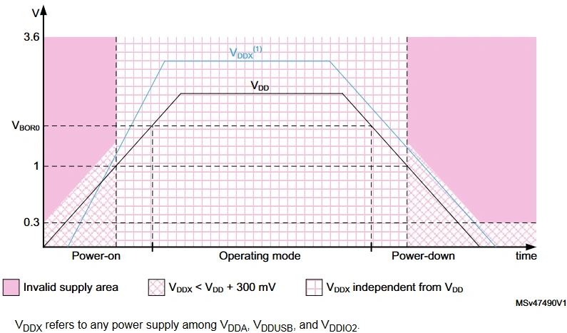
STM32U575 power-up and power-down sequence showing VDD, VDDX invalid supply area, and VDDIO2 independent domain constraints
The VDDIO2 supply domain powering Port G is a significant architectural change from the STM32L476, where all I/O ports shared the main VDD rail (with VDDIO2 only used for select Port G pins). On the STM32U575, VDDIO2 can be set to a voltage different from VDD, enabling direct 1.8 V I/O interfacing with external processors, sensors, or memory devices without level shifters. If your design does not require voltage translation, connect VDDIO2 directly to VDD with a dedicated 100 nF decoupling capacitor. Do not leave VDDIO2 floating — an unpowered VDDIO2 causes Port G pins to remain in an undefined state regardless of firmware configuration.
The STM32U575's dual 14-bit ADC architecture represents the highest analog resolution available in the STM32 ultra-low-power family. Achieving the full 14-bit performance in practice requires careful attention to both schematic pin assignment and PCB routing — the analog subsystem is the most noise-sensitive area of any mixed-signal design.
| Analog Resource | Pins (LQFP64) | Pins (LQFP144) | Key Specifications |
|---|---|---|---|
| ADC1 channels | PC0–PC5, PA0–PA7, PB0–PB1 (IN1–IN16) | All LQFP64 channels + PF3, PF4 (IN18–IN19) | 14-bit resolution, up to 5.33 Msps, oversampling up to 256× |
| ADC2 channels | PC0–PC1, PC4–PC5, PA0–PA7, PB0–PB1 (shared with ADC1 on same pins) | Adds PF5, PF10 (IN19–IN20) | 14-bit, 5.33 Msps, fully independent from ADC1 for simultaneous sampling |
| DAC1 OUT1 | PA4 | PA4 | 12-bit, output buffer or unbuffered mode, can drive COMP or OPAMP input |
| DAC1 OUT2 | PA5 | PA5 | 12-bit, same specs as DAC1_OUT1 |
| OPAMP1 INP | PA0, PA3, PB0 (selectable) | PA0, PA3, PB0 | Internal or external input selection; output to PA1 or internal ADC |
| COMP1 INP | PA1, PC4, PB2 (selectable) | PA1, PC4, PB2 | Low-power comparator, 60 ns propagation delay |
| COMP2 INP | PA7, PB4 (selectable) | PA7, PB4 | Shares VREFINT DAC as reference; output routable to TIM1_BKIN |
| VREF+ | Shared with VDDA on LQFP64 | Dedicated Pin 23 on LQFP144 | ADC full-scale reference; use external precision reference on LQFP144 for 14-bit accuracy |
Figure 4: STM32U575 internal VREFBUF block diagram showing VREFINT buffered output path to VREF+ pin with selectable output impedance trim resistors and external decoupling capacitor connection to VSSA

As shown in the VREFBUF block diagram above, the STM32U575 includes an internal voltage reference buffer that drives the VREF+ pin from VREFINT without requiring an external precision reference IC. The buffer output impedance is selectable via trim resistors to balance between output drive strength and power consumption. When using the internal VREFBUF, a minimum 1 µF external capacitor must be placed directly on the VREF+ pin to VSSA to ensure buffer stability — without this capacitor the buffer may oscillate, directly corrupting ADC conversion results. For the highest ADC accuracy, bypass the internal VREFBUF entirely and drive VREF+ from a dedicated external precision voltage reference instead.
The most impactful schematic decision for ADC accuracy on the STM32U575 is the choice of package. The LQFP64 combines VREF+ and VDDA onto a single physical pad, meaning the ADC reference is directly polluted by analog bias current transients from the OPAMP and DAC circuits sharing the same supply. For any application requiring more than 12 effective bits of ADC accuracy, select the LQFP144 or UFBGA169 and drive the dedicated VREF+ pin from a standalone precision voltage reference with its own LC filter and dedicated ground return to VSSA.
The STM32U575 combines higher operating frequency (160 MHz vs. 80 MHz on STM32L4), wider data buses (OCTOSPI vs. QSPI), and a USB-C Power Delivery controller (UCPD) — all of which introduce layout constraints not present in previous generation designs. The guidelines below address the U575-specific requirements beyond the general STM32 layout rules covered in the STM32 Pinout and Package Guide.
For PCB assembly of STM32U575 designs, request X-ray inspection for BGA variants (UFBGA169) and automated optical inspection (AOI) verification of all 0.5 mm pitch LQFP solder joints. Fine-pitch LQFP packages at 0.5 mm are at the practical limit of manual solder inspection reliability.
NextPCB supports the full manufacturing lifecycle for STM32U575-based designs across all package variants.
Not directly. While both families are available in LQFP64 and LQFP144 packages at 0.5 mm pitch, the pin assignments differ significantly. Key differences include the introduction of VDDIO2 as a dedicated supply for Port G (requiring a new power rail on the PCB), the BOOT0 hardware pin present on U575 but option-byte controlled on some L4 variants, and entirely different alternate function mappings for shared peripherals. A pin-to-pin compatibility check in STM32CubeMX against both part numbers is required before attempting a drop-in substitution.
The STM32U585 adds a hardware Neural Processing Unit (NPU) — specifically, an Arm Cortex-M55 with Helium SIMD extensions and a dedicated 512 KB SRAM for ML inference. All other specifications, package options, pinout, and peripheral set are identical to the STM32U575. The two parts are fully pin-compatible and share the same PCB footprint. If your application may require on-device ML inference in future firmware revisions, select the U585 during initial design to avoid a board spin.
On the STM32U575, BOOT0 is a dedicated hardware input pin (unlike the STM32L432 where boot mode is controlled purely via option bytes). Pull BOOT0 to VSS through a 10 kΩ resistor for normal Flash boot. Add a test point or footprint for a zero-ohm jumper to allow BOOT0 to be pulled high for DFU bootloader entry during production programming or firmware recovery. Do not leave BOOT0 floating — the internal pull-down may not be sufficient to prevent inadvertent bootloader entry in high-noise environments.
Yes, this is a supported configuration. VDDIO2 can be set independently of VDD within its range of 1.08 V to 3.6 V, enabling direct interfacing of Port G pins to 1.8 V logic devices without external level shifters. Ensure that the VDDIO2 rail is powered before or simultaneously with VDD — Port G pins must not be driven externally before VDDIO2 is active, as this can cause current injection through the I/O clamping diodes. Configure the GPIO speed and output type for Port G pins appropriately in firmware for the 1.8 V domain — the maximum toggle frequency is reduced at lower supply voltages.
The most common root cause is unmatched trace lengths among the eight data lanes, clock, and chip select. At 100 MHz DDR, a 50 mil length difference between data lanes introduces approximately 8.5 ps of skew, which is significant relative to the setup and hold window at this frequency. Verify your length matching in the PCB layout tool before assembly. The second common cause is operating the OCTOSPI clock before the external device's power supply has stabilized — add a firmware delay after VDD reaches its target voltage before issuing the first OCTOSPI transaction. The third cause is missing termination: add a 22–33 Ω series resistor on the CLK and each IO line close to the MCU pins to dampen ringing on unmatched transmission lines.
The crystal load capacitance (CL) is specified in the crystal datasheet. The PCB capacitors C1 and C2 (placed on OSC_IN and OSC_OUT) must satisfy CL = (C1 × C2) / (C1 + C2) + Cstray, where Cstray is the parasitic capacitance of the PCB traces and MCU input pins (typically 3–5 pF total). For a crystal with CL = 12 pF and Cstray = 4 pF, symmetric load capacitors of C1 = C2 = 16 pF will achieve the target. Use C0G/NP0 ceramic capacitors in 0402 package for temperature stability. Incorrect load capacitance causes frequency offset, which propagates directly into USB SOF timing errors and UART baud rate inaccuracy.
The gap between theoretical resolution and effective number of bits (ENOB) on the STM32U575 ADC almost always originates from one of four sources. First, VDDA is not isolated from VDD switching noise — verify the ferrite bead is installed in series between VDD and VDDA and check its impedance at 100 MHz is at least 600 Ω. Second, VREF+ and VDDA are shared (LQFP64 only) — upgrade to LQFP144 for dedicated VREF+ access. Third, the ADC sampling time is too short for the source impedance of the connected sensor — increase the sampling cycles in STM32CubeMX. Fourth, the ADC input trace runs in parallel with a digital switching signal — reroute the analog input to the analog side of the PCB partition, away from all toggling GPIO and SPI/I²C lines.

Still, need help? Contact Us: support@nextpcb.com
Need a PCB or PCBA quote? Quote now

