
 Surface


Julia Wu - Senior Sales Engineer at NextPCB.com

 NextPCB Capabilities
Printed Circuit Boards
NextPCB Capabilities
Printed Circuit Boards
 PCB Assembly
 Layer Buildup
 SMD-Stencils
 PCB Design-Aid & Layout
 Mechanics
 Quality
 Drills & Throughplating
 Factory & Certificate
 PCB Assembly Factory Show
Certificate
PCB Assembly Factory Show
Certificate
Support Team
Feedback:
support@nextpcb.com


In modern high-speed, high-density interconnect (HDI) embedded system designs, the microcontroller (MCU) functions not only as the computing brain but also as the absolute physical boundary of printed circuit board (PCB) design. Every pinout allocation directly governs Signal Integrity (SI), Power Integrity (PI), and Design for Manufacturability (DFM).
This guide analyzes the ultra-low-power, high-performance STM32L476 series (spanning LQFP-64 to LQFP-144 packages). We detail critical layout checklists, including pinout configurations, Power Delivery Network (PDN) routing (SMPS vs. LDO), exposed thermal pad requirements, and trace impedance matching constraints to ensure first-pass prototype success.
* Core Hardware Engineering Resources:
Before starting any schematic symbol generation or physical board layout, always consult the official electrical characteristics, alternate function mappings, and mechanical package tolerance dimensions. You can access the official document here:
Download STM32L476xx Official Datasheet (PDF) (Resource provided by HQ Online)
STM32 is a comprehensive portfolio of 32-bit microcontrollers (MCUs) developed by STMicroelectronics, built upon ARM® Cortex®-M processors. If a fully assembled PCB assembly (PCBA) represents the body of an electronic device, the STM32 acts as the central brain—processing sensor data, driving peripheral interfaces, and running control algorithms.
With an extensive software ecosystem (including STM32CubeMX, HAL libraries), competitive pricing, and robust pin-to-pin compatibility, STM32 is the industry-standard choice for embedded system designs globally.
High-speed MCUs utilize multiple isolated power domains to optimize efficiency and minimize noise coupling. Specifically, the core logic power, analog peripherals (VDDA), and specific I/Os (VDDIO2, VDDUSB) operate on distinct rails.
The hardware designer must prevent electrical overstress or latch-up events when these power domains ramp up or down. Standard silicon architectures dictate that external analog and digital peripheral supply rails (VDDX) must follow strict relative voltage limits relative to the main VDD digital rail.
Image 1. Power-up/down sequence
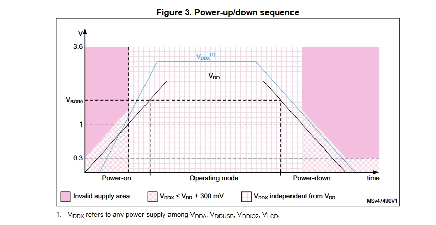
As illustrated in Figure 3: Power-up/down sequence, the pink-shaded zone represents the "Invalid supply area" where the chip's internal reset state cannot be guaranteed. The cross-hatched area mandates that VDDX must remain below VDD + 300 mV during power transitions to prevent parasitic body-diode conduction.
During the design lifecycle, engineers frequently transition from prototyping packages (like LQFP-144) to cost-optimized mass production packages (like LQFP-64) without changing core firmware. However, minor variations in chip pinout suffixes can lead to major hardware layout revisions.
Even within the exact same LQFP-144 mechanical outline, the physical pin assignments differ radically depending on whether the design leverages the integrated Low Dropout (LDO) regulator or the high-efficiency external Switch-Mode Power Supply (SMPS) power tree.
Image 2: STM32L476Zx LQFP144 pinout
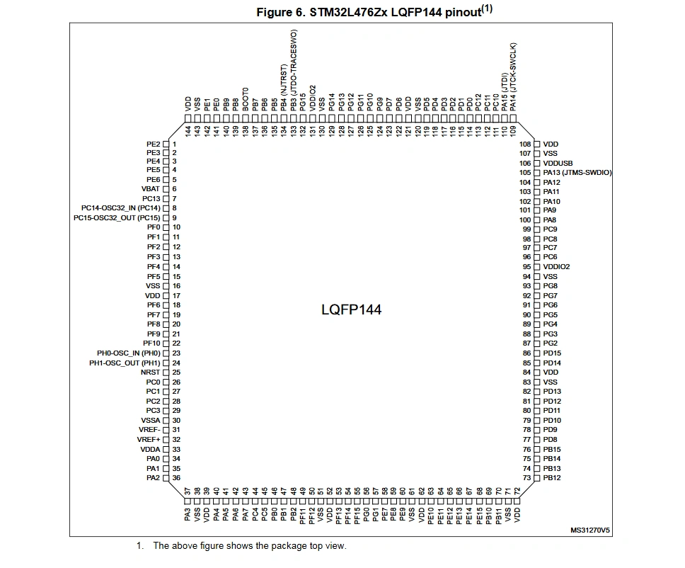
Figure 6 (Image 2) displays the standard LQFP-144 pin distribution, providing up to 114 general-purpose I/O (GPIO) pins, where power distribution relies on traditional VDD and VSS pairs.
Image 3: STM32L476Zx, external SMPS device, LQFP144 pinout
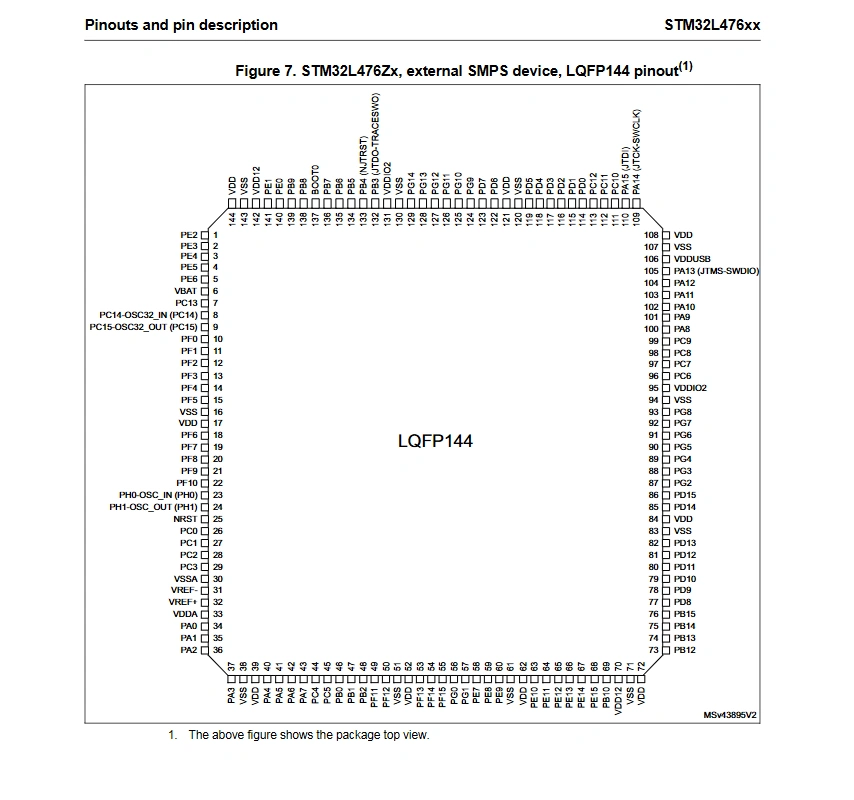
By contrast, Figure 7 (Image 3) highlights the pin configuration for the SMPS-dedicated LQFP-144 package. Notice the introduction of VDD12 pins (such as Pin 71 and Pin 142) which replace standard power pins to accept external, highly efficient low-voltage step-down supply rails.
To achieve ultra-low dynamic run currents (often below 100 µA/MHz), STM32L476 series devices support two primary internal core voltage supply schemes: an internal Linear LDO Regulator or an External Switch-Mode Power Supply (SMPS).
Image 4: Current consumption measurement scheme with and without external SMPS power supply
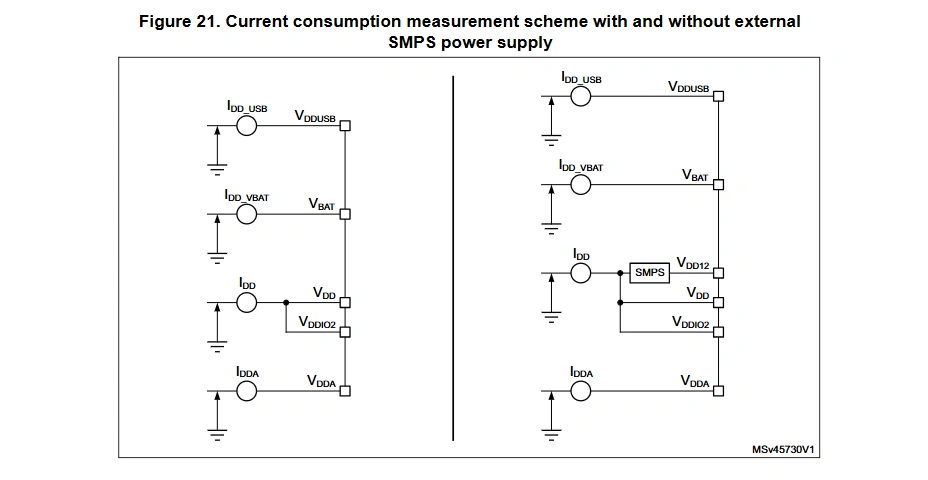
As documented in Figure 21 (Image 4), the standard power configuration (left) utilizes internal regulators to step down the external VDD/VDDIO2 rails to the core digital domain. The external SMPS configuration (right) routes the external VDD supply through an external buck regulator (inductor and filter capacitor network) to feedback directly to the VDD12 terminal.
To capture accurate readings from high-impedance sensors using the onboard Analog-to-Digital Converter (ADC), the internal reference voltage must remain immune to system-level noise and thermal fluctuations.
Image 5: VREFINT versus temperature
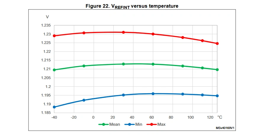
According to Figure 22 (Image 5), the internal base reference voltage VREFINT exhibits flat temperature coefficient characteristics, staying extremely stable within a nominal window of 1.19 V to 1.23 V over the entire -40°C to +120°C industrial operating range.
For packages featuring an exposed center metal ground pad (such as QFN or WLCSP configurations), the thermal pad serves as both the lowest impedance path to system ground and the primary thermal dissipation pipeline.
When routing fast switching signals, traces act as transmission lines rather than simple DC paths. Trace geometries must be strictly controlled to maintain target characteristic impedances.
     Microstrip Line (Top Layer)               Stripline (Internal Layer)

        [ Trace Width W ]                         ================== (Reference Ground Plane)
      =====================                       \  Dielectric H1 /
      \   Dielectric H    /                        ================= (Inner Signal Trace W)
    ========================= (Ground Plane)      /  Dielectric H2 \
                                                  ================== (Reference Ground Plane)
Achieving a reliable, first-pass functional design requires aligning the physical layout with supply-chain realities at the onset of the project.
If you are moving from schematic to physical layout for your STM32L476-based design, NextPCB provides the full-stack manufacturing and engineering support to take your board from prototype to production.
No. Even within the identical LQFP-144 mechanical outline, the pin assignments differ significantly between standard LDO variants and SMPS-enabled variants. For example, the SMPS package introduces dedicated VDD12 pins at positions that carry standard power functions on the LDO package. Always cross-reference the exact ordering suffix (e.g., STM32L476ZGT6) against the official datasheet pin table before generating your schematic symbol or PCB footprint.
Place a 100 nF ceramic capacitor (X5R or X7R, 0402 package) within 0.5 mm of every VDD and VDDA pin, with direct routing to the nearest ground via. For bulk decoupling, add one 4.7 µF or 10 µF capacitor per power domain cluster. The VDDA analog supply should additionally use a ferrite bead filter in series from the main 3.3 V rail to isolate switching noise from the ADC reference path.
Choose the external SMPS path when your application targets run currents below 100 µA/MHz or when operating from a battery where energy budget is critical. The SMPS topology routes core voltage through an external buck inductor and filter network to VDD12, achieving significantly higher efficiency at light loads compared to the internal LDO. The trade-off is added BOM cost, more complex layout rules around the switching node, and the requirement to source an SMPS-pinout variant of the STM32L476.
Use a segmented stencil aperture — typically a 3×3 or 4×4 grid pattern — covering 50% to 75% of the total thermal pad area. This creates outgassing channels that let trapped flux volatiles escape during reflow rather than forming voids. Additionally, keep thermal via diameters between 0.2 mm and 0.3 mm; oversized vias cause solder siphoning through capillary action, reducing joint integrity and thermal conductance to the ground plane.
The most frequent root causes are: (1) length mismatch between USB_DM and USB_DP exceeding ±5 mil, (2) routing the pair over a split in the adjacent ground reference plane, which spikes trace impedance and injects common-mode noise, (3) differential impedance deviating from the 90 Ω ±10% target due to incorrect trace width or spacing relative to the actual fabricated stackup, and (4) insufficient ground stitching vias near layer transition points. Request an impedance-controlled stackup report from your fabrication partner before finalizing trace geometry.
If both rails share the same 3.3 V nominal voltage, the simplest and most reliable approach is to connect them to a single unified power plane. Rail isolation for noise reasons should be implemented with a ferrite bead rather than discrete regulators — this inherently guarantees zero voltage skew between the rails during power-up and power-down transitions. If you must use separate regulators, use a supervisory IC or power sequencer to enforce that VDDX never exceeds VDD + 300 mV during any transient condition.
Standard LQFP-64 and LQFP-144 packages do not have an exposed thermal pad, so via-in-pad is generally not required for the MCU footprint itself. VIPPO becomes necessary when routing high-density fanout in tight HDI designs where vias must land inside SMT pads of surrounding passive components or connectors. If your design does include QFN or WLCSP variants of other ICs, specify VIPPO explicitly in your fabrication notes, as it requires epoxy fill, copper plating, and surface planarization steps not included in standard PCB manufacturing.

Still, need help? Contact Us: support@nextpcb.com
Need a PCB or PCBA quote? Quote now

