
 Surface


Arya Li, Project Manager at NextPCB.com

 NextPCB Capabilities
Printed Circuit Boards
NextPCB Capabilities
Printed Circuit Boards
 PCB Assembly
 Layer Buildup
 SMD-Stencils
 PCB Design-Aid & Layout
 Mechanics
 Quality
 Drills & Throughplating
 Factory & Certificate
 PCB Assembly Factory Show
Certificate
PCB Assembly Factory Show
Certificate
Support Team
Feedback:
support@nextpcb.com


In the world of advanced electronics—from aerospace avionics to compact medical wearables—Rigid-Flex PCB Assembly represents the pinnacle of interconnect technology. It is not merely about connecting components; it is about creating a 3D interconnect system that saves space, reduces weight, and improves mechanical reliability by eliminating connectors.
However, assembling a Rigid-Flex board is significantly more complex than the standard process. It introduces unique challenges regarding moisture control, thermal management, and mechanical fixturing.
At NextPCB, we specialize in high-reliability PCB assembly services, bridging the gap between complex designs and mass production. This guide provides a deep dive into the Rigid-Flex assembly process, offering actionable DFM (Design for Manufacturing) insights for engineers and procurement managers.
Before diving into the assembly line, it is crucial to understand the substrate you are working with. A Rigid-Flex PCB integrates rigid circuit board elements (typically FR-4) with flexible circuits (Polyimide) into a single, permanently bonded unit.
Decision Tip: Are you unsure if you truly need a complex Rigid-Flex structure, or if a standard Rigid board with discrete flex cables would suffice? Read our comprehensive comparison: Flex vs. Rigid vs. Rigid-Flex PCB: Making the Right Choice.
If you have determined that Rigid-Flex is the right solution for your 3D packaging needs, the focus now shifts to manufacturability.
Compared to the standard rigid PCB assembly process, the rigid-flex process introduces variables that, if uncontrolled, can lead to catastrophic failure.

Polyimide (PI), the core material of the flexible section, is highly hygroscopic. It absorbs moisture from the air much faster than FR-4—up to 3% by weight. During the high temperatures of reflow soldering (240°C - 260°C), trapped moisture turns into steam, expanding rapidly and causing delamination (layer separation) or "popcorning."
Flexible zones make the board unstable. Standard SMT conveyors cannot handle a floppy board.
While the logic is similar to general assembly—which you can explore in our comprehensive guide to PCB assembly—the specific steps for Rigid-Flex differ significantly to accommodate material properties.
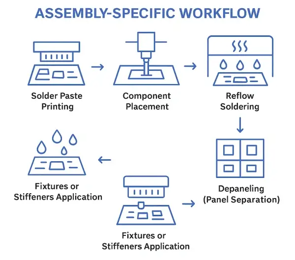
Our CAM engineers review the "Transition Zone" (where rigid meets flex). Vias placed too close to the transition line are a major failure point.
As mentioned, this is a critical step for material stability. The baking time is calculated to ensure the PI material is sufficiently dry before hitting the reflow oven, reducing the risk of internal stress or layer separation.
The board is mounted on a supportive carrier. We utilize Surface Mount Technology (SMT) to place components.
Note: For optimal assembly reliability, we recommend prioritizing the placement of high-density or complex components (such as fine-pitch BGAs) on the rigid sections. If components must be placed on the flexible areas, they should be supported by a proper stiffener design to prevent mechanical stress on the solder joints.
Because Polyimide transfers heat differently than FR-4, the thermal ramp-up must be carefully controlled to prevent thermal shock to the adhesive layers. We use specialized reflow profiles with a slower soak zone to ensure even heating across both rigid and flex materials.
Unlike rigid boards that can be V-cut (scored), rigid-flex boards require more precise methods. We recommend low-stress depaneling techniques, such as precision routing or laser cutting, to minimize the risk of damage to the flexible coverlay and the sensitive transition zones.
To ensure your Rigid-Flex design sails through production, conducting a thorough DFM (Design for Manufacturability) review is essential. Consider these critical design rules:
If you are placing components on a flexible arm, you must utilize a stiffener (FR-4, PI, or Stainless Steel) on the opposite side. Without a stiffener, the solder joints will crack when the flex bends.
Never place plated through-holes (PTH) or vias strictly within the bend line or the transition zone.
To maximize dynamic flex life (according to IPC-2223):
Do not ship rigid-flex boards as loose pieces. Supply them in a panel array.
We often hear from procurement managers: "Why is Rigid-Flex assembly more expensive?"
The cost is driven by:
However, the Total Cost of Ownership (TCO) is often lower. By using Rigid-Flex, you eliminate:
Rigid-Flex assembly is not just about having SMT machines; it is about process discipline. At NextPCB, we combine over 15 years of manufacturing data with advanced assembly protocols.
Q1. Why do rigid‑flex PCBs often fail electrical continuity after assembly or show high resistance/open circuits?
Answer: Rigid‑flex boards combine rigid and flexible sections, and design or material issues can lead to trace stress, conductor fractures, or delamination in flex zones. When the flex regions aren’t designed with adequate bend relief or correct stack‑up (e.g., improper dielectric or adhesive selection), copper traces can stress and crack, leading to intermittent or open circuits after assembly or thermal cycling.
Q2. What specific design challenges cause rigid‑flex assemblies to fail mechanically (e.g., bends, cracks, or stress at rigid‑flex interfaces)?
Answer: Rigid‑flex PCBs require special attention to bend radius, material selection, and layer transitions. Inappropriate bend radius or placing vias too close to flex/rigid boundaries increases mechanical stress during assembly or use, leading to fractures or delamination under repeated bending or vibration.
Q3. Why do rigid‑flex PCB designs often cost much more and have longer prototype lead times than standard rigid PCBs?
Answer: Rigid‑flex boards use complex laminate materials, multi‑stage lamination processes, controlled stack‑ups, and precise drilling/plating across rigid and flex regions. These specialized processes require more time, careful DFM/DFT planning, and skilled engineering support to avoid manufacturing defects.
Q4. How do component placement and bending design affect rigid‑flex PCB assembly reliability?
Answer: Placing components too close to a bend or flex section can cause solder joint cracking or pad delamination when the PCB bends or undergoes thermal stress. Proper placement away from flexing areas and the use of stiffeners to reinforce components are key to prevent assembly failures.
Q5. What are the most common DFM (Design for Manufacturability) mistakes that lead to rigid‑flex PCB assembly problems?
Answer: Rigid‑flex design introduces unique DFM constraints compared to rigid PCBs. Common missteps include: placing vias too close to flex boundaries, incorrect material choice, insufficient conductor spacing, failure to honor minimum bend radius, overlapping traces in bend zones, and inadequate drill‑to‑copper spacing.
Rigid-Flex technology is the future of compact, high-performance electronics. Don't let assembly challenges hold your design back.
Request a Free Quote Today and let our engineering team review your Gerber files for optimal manufacturability.

Still, need help? Contact Us: support@nextpcb.com
Need a PCB or PCBA quote? Quote now

