
 Surface


Lolly Zheng- Sales Account Manager at NextPCB.com

 NextPCB Capabilities
Printed Circuit Boards
NextPCB Capabilities
Printed Circuit Boards
 PCB Assembly
 Layer Buildup
 SMD-Stencils
 PCB Design-Aid & Layout
 Mechanics
 Quality
 Drills & Throughplating
 Factory & Certificate
 PCB Assembly Factory Show
Certificate
PCB Assembly Factory Show
Certificate
Support Team
Feedback:
support@nextpcb.com


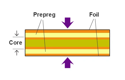
In the rapidly evolving world of electronics hardware, the printed circuit board (PCB) is no longer just a holder for components; it is a critical active component of the circuit design itself. With the rise of high-speed digital interfaces (like PCIe Gen 5/6), 5G/6G communication, and dense IoT devices, understanding the fundamental building blocks of a PCB manufacturing stackup—Core, Prepreg, and Copper Foil—is essential for every hardware engineer and procurement manager.
A poorly designed stackup can lead to signal integrity issues (crosstalk, impedance mismatch), warping during reflow soldering, and unnecessary cost overruns. Whether you are prototyping a simple IoT sensor or a complex turnkey PCB project for automotive applications, selecting the right combination of materials is the first step toward product success.
At NextPCB, we have optimized our fabrication processes to meet 2026 industry standards, ensuring that your boards are not only low cost PCB solutions but also meet IPC Class 2 and Class 3 reliability requirements.
The Core is the fundamental "backbone" of your PCB. In technical terms, a core is a fully cured (C-Stage) fiberglass-epoxy laminate with copper bonded to one or both sides. Think of it as a "double-sided PCB" in its simplest raw form.
In modern designs, the Dielectric Constant (Dk) and Dissipation Factor (Df) of the core are vital for calculating characteristic impedance and ensuring lower insertion loss at high frequencies. Below are the standard core specifications used at NextPCB:
| Core Type (mm) | Dielectric Thickness (mm) | Copper Weight (oz) | Top/Bottom Copper (mm) | Dielectric Constant (Dk) |
|---|---|---|---|---|
| 0.135 (H/H) | 0.103 | 0.5 oz | 0.016 / 0.016 | 4.2 |
| 0.15 (H/H) | 0.118 | 0.5 oz | 0.016 / 0.016 | 4.2 |
| 0.17 (1/1) | 0.106 | 1.0 oz | 0.032 / 0.032 | 4.2 |
| 0.2 (1/1) | 0.136 | 1.0 oz | 0.032 / 0.032 | 4.2 |
| 0.2 (H/H) | 0.168 | 0.5 oz | 0.016 / 0.016 | 4.2 |
| 0.2 (2/2) | 0.076 | 2.0 oz | 0.062 / 0.062 | 4.2 |
| 0.4 (1/1) | 0.336 | 1.0 oz | 0.032 / 0.032 | 4.2 |
| 0.5 (1/1) | 0.436 | 1.0 oz | 0.032 / 0.032 | 4.5 |
| 0.8 (1/1) | 0.736 | 1.0 oz | 0.032 / 0.032 | 4.5 |
| 1.0 (1/1) | 0.936 | 1.0 oz | 0.032 / 0.032 | 4.5 |
| 1.2 (1/1) | 1.136 | 1.0 oz | 0.032 / 0.032 | 4.5 |
| 1.6 (1/1) | 1.536 | 1.0 oz | 0.032 / 0.032 | 4.5 |
| 2.0 (1/1) | 1.936 | 1.0 oz | 0.032 / 0.032 | 4.5 |
Note: Copper thickness values listed above are nominal. Final copper thickness may vary after plating and etching processes.
For high-performance applications where insertion loss is a critical constraint, standard FR-4 cores might be replaced with Low-Df materials like Rogers or Isola to maintain signal integrity at multi-gigahertz speeds.
Prepreg (short for "Pre-impregnated") is the insulation layer that binds cores and copper foils together. Unlike the core, Prepreg is "B-Stage" material. This means the fiberglass is impregnated with resin but is only partially cured.
Professional engineers select prepreg not just by thickness, but by "Glass Weave Style" and "Resin Content (RC)." This directly affects the Dielectric Constant (Dk), which is crucial for PCBA signal integrity.
| Glass Style | Dielectric Thickness (mm) | Resin Content (RC %) | Dielectric Constant (Dk) | Application |
|---|---|---|---|---|
| 106 | 0.05 | 73% | 4.0 | Laser drilling, fine pitch HDI. |
| 1080L | 0.068 | 63% | 4.0 | Thin dielectric, low profile designs. |
| 1080 | 0.077 | 67% | 4.0 | Standard high-speed signal gaps. |
| 1080H | 0.09 | 71% | 4.0 | High resin flow requirements. |
| 2313 | 0.103 | 61% | 4.2 | General purpose, stable Dk. |
| 2116 | 0.125 | 57% | 4.2 | Balanced resin flow and thickness. |
| 1506 | 0.16 | 48% | 4.1 | Medium thickness (non-standard). |
| 7628 | 0.2 | 48% | 4.5 | Thick dielectric, cost-effective. |
| 7628H | 0.23 | 53% | 4.5 | High resin version of 7628. |
Note: Dk values are typical at 1GHz frequency. For 2026 high-frequency designs, Dk and Df (Dissipation Factor) are key metrics for achieving lower insertion loss.
While both are composed of similar base materials (Fiberglass + Resin), their function in the PCBA (PCB Assembly) ecosystem is distinct:
The copper foil acts as the conductive pathway for your signals. In modern quick turn PCB fabrication, we typically encounter two main forms:
Pro Tip for 2026 Designs: For high-speed signals (10Gbps+), the surface roughness of standard copper can cause signal loss. Engineers should request VLP (Very Low Profile) or HVLP (Hyper Very Low Profile) copper foil to minimize insertion loss and improve high-speed data integrity.
Available thicknesses at NextPCB include:
Note: All copper weights are nominal; final thicknesses may fluctuate slightly due to the etching and plating cycles required for circuit definition.
To ensure your low cost PCB stays within budget without sacrificing quality, follow these Design for Manufacturing (DFM) rules:
Always maintain symmetry in your stackup (e.g., layer 2 matches layer 5 in a 6-layer board) regarding copper thickness and Prepreg type. Asymmetrical stackups cause warping (bow and twist) during the high temperatures of PCB assembly reflow, leading to defective solder joints.
Mixing materials (e.g., FR4 Core with Rogers Prepreg) is possible but requires specialized lamination cycles. This increases cost and lead time. Consult NextPCB engineers early if you need high-frequency materials for lower insertion loss at high frequencies.
Designing a stackup that relies on obscure prepreg thicknesses can delay your quick turn PCB order. Stick to standard weaves (1080, 2116, 7628) whenever possible. Using standard stackups also improves yield consistency in mass production.
As a leading reliable manufacturer, NextPCB provides comprehensive solutions from prototype to mass production. Our 2026 capabilities feature:
If you are unsure about your stackup, use our Free Stackup Builder tool or upload your Gerber files for a complimentary DFM check by our engineering team.
Get Instant Quote & Free DFM Check Get Instant Quote & Free DFM Check
A: Yes, this is common. For example, stacking two sheets of 1080 prepreg to achieve a specific thickness for impedance control. However, we generally avoid stacking more than 3 sheets to reduce the risk of measling, resin voids, and thickness inconsistency.
A: FR4 is a woven glass epoxy (suitable for multilayer boards). CEM-1 is a composite of paper core and glass surface (cheaper, but usually limited to single-sided PCBs). For professional electronics, NextPCB recommends FR4.
A: Yes. We call this the "pressed thickness." The resin flows into the copper gaps of the adjacent layers. NextPCB’s engineering software calculates this automatically to ensure your 50Ω impedance traces are accurate.
A: Custom stackups may require non-standard material stock or extra lamination cycles. Using our "Standard Stackup" options is the best way to achieve a low cost PCB and maintain high production yields.
Ready to start your next project? Trust NextPCB for reliable, high-quality manufacturing.

Still, need help? Contact Us: support@nextpcb.com
Need a PCB or PCBA quote? Quote now

