
 Surface


Zhang

 NextPCB Capabilities
Printed Circuit Boards
NextPCB Capabilities
Printed Circuit Boards
 PCB Assembly
 Layer Buildup
 SMD-Stencils
 PCB Design-Aid & Layout
 Mechanics
 Quality
 Drills & Throughplating
 Factory & Certificate
 PCB Assembly Factory Show
Certificate
PCB Assembly Factory Show
Certificate
Support Team
Feedback:
support@nextpcb.com


In the world of PCB manufacturing, precision defines performance. PCB milling (also known as CNC routing) is the mechanical process of removing specific areas of the copper-clad laminate to form the board's outline, internal cutouts, and slots. Unlike chemical etching which defines the traces, milling defines the physical shape of your printed circuit board.
For hardware engineers and procurement managers, understanding the milling process is critical. A poorly defined mechanical layer can lead to dimensional errors, assembly failures during PCBA (PCB Assembly), or costly production delays. In 2025, with electronic devices becoming smaller and enclosures becoming tighter, the tolerance requirements for PCB milling have tightened significantly—often requiring accuracy within ±0.1mm.
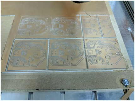
When finalizing your design for production, you generally have two options for separating individual boards from the manufacturing panel: Milling (Routing) or V-Scoring.
V-scoring involves cutting a "V" shaped groove on the top and bottom of the PCB, leaving a thin web of material remaining. This is ideal for:
Milling uses a rotating cutting tool (router bit) to cut through the board completely. This is the standard choice for:
Pro Tip: For high-volume turnkey PCB orders, NextPCB often recommends a combination: milling for the intricate features and V-scoring for the straight panel edges to optimize both cost and stability.
The success of the milling process depends entirely on the data provided in your Gerber files. The "Mechanical Layer" (often GKO, GM1, or Outline layer) acts as the blueprint for the CNC machine.
To ensure your board is manufactured correctly by NextPCB's engineering team, your mechanical layer must contain:
Unlike etching data where linewidth matters, milling data is interpreted as a path. Most PCB manufacturing CAM systems interpret the line in your mechanical layer as the center of the router bit's path. However, professional fabricators like NextPCB will automatically apply "tool compensation" to cut along the outside of your line to ensure the final board dimensions match your design exactly.
To avoid "Engineering Questions" (EQ) delays and ensure a smooth transition to PCB assembly, follow these DFM (Design for Manufacturing) guidelines:
The standard routing bit diameter in the industry is 2.0mm (approx. 79 mil).
Keep copper features (traces, pads, planes) away from the milling path. Cutting through copper can cause:
Recommended Clearance: ≥ 0.25mm (10 mil) from the board edge or cutout edge.
Internal milling is often used for mounting holes, ventilation, or high-voltage isolation (creepage).
Since a round router bit cannot cut a perfect 90° square corner, creating a rectangular slot results in rounded corners. If you are inserting a rectangular component (like a USB connector or a fuse holder) into the slot, it might not fit.
Solution: Use "Dog Bone" corners (drilling over-sized holes in the corners) to create clearance for the component's sharp edges.
Clearly distinguish between Plated Through Slots (PTS) and Non-Plated Slots (NPTS) in your mechanical layer. PTS requires milling before the plating process, while NPTS is done after. Ambiguity here is a top cause of scrapped boards.
While standard outline milling is included in the base price, complex milling can influence the cost of your low cost PCB strategy.
At NextPCB, we optimize the routing path during our CAM review to provide the most competitive pricing without sacrificing quality.
A: Not with standard milling. The only way to achieve a true 90° internal corner is to use a secondary process like laser cutting or punch pressing (for high volumes), but "Dog Bone" reliefs are the standard engineering solution.
A: We can mill slots as narrow as 0.8mm (using a 0.8mm bit). For slots narrower than this, we recommend treating them as a series of overlapping drill holes (nibbling) or reviewing the design.
A: Indirectly, yes. The panelization method (tab-route vs. V-score) affects how the PCBA rails hold the board. Proper milling design ensures the boards don't flex or break away prematurely during the SMT placement process.
PCB milling is more than just cutting a shape; it is the foundation of mechanical integration for your product. Whether you are building a simple prototype or a complex high-frequency aerospace board, the accuracy of the mechanical layer is paramount.
Why Partner with NextPCB?
Ready to bring your design to life? Upload your Gerber files today for an instant DFM check and quote.

Still, need help? Contact Us: support@nextpcb.com
Need a PCB or PCBA quote? Quote now

