
 NextPCB Capabilities
Printed Circuit Boards
NextPCB Capabilities
Printed Circuit Boards
 PCB Assembly
 Layer Buildup
 SMD-Stencils
 PCB Design-Aid & Layout
 Mechanics
 Quality
 Drills & Throughplating
 Factory & Certificate
 PCB Assembly Factory Show
Certificate
PCB Assembly Factory Show
Certificate
Support Team
Feedback:
support@nextpcb.com


The past several decades have seen the development of integrated circuit (IC) packages, which are the enclosures that protect and provide a connection point for integrated circuits. IC packages enable the construction of complex and reliable electronic devices, from the simplest of resistors and capacitors to the most complex of microprocessors. In this article, we will explore the various types of IC packages, as well as the advantages and disadvantages of each type. We will also discuss the essential elements of an IC package, such as its size, shape, and material composition. We will also discuss the various methods of IC package I/O termination, such as peripheral, grid-array, ball-grid array, and flip-chip. Finally, we will review some of the best practices for selecting and using IC packages in order to maximize their effectiveness.
An IC package is a physical package that houses an integrated circuit (IC). It contains the IC, leads, and other components needed to connect the IC to a circuit. IC packages come in a range of shapes, sizes, and types. Common IC package types include quad flat packs (QFPs), dual inline packages (DIPs), and ball grid arrays (BGAs). The type of package chosen for an IC depends on the application and the requirements of the circuit.
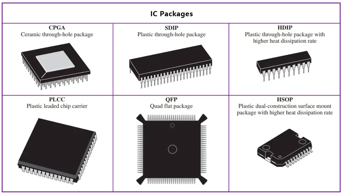
There are several different types of IC packages, each of which has its own advantages and disadvantages. The most common types of IC packages are through-hole packages, surface-mount packages, and pin grid array packages.
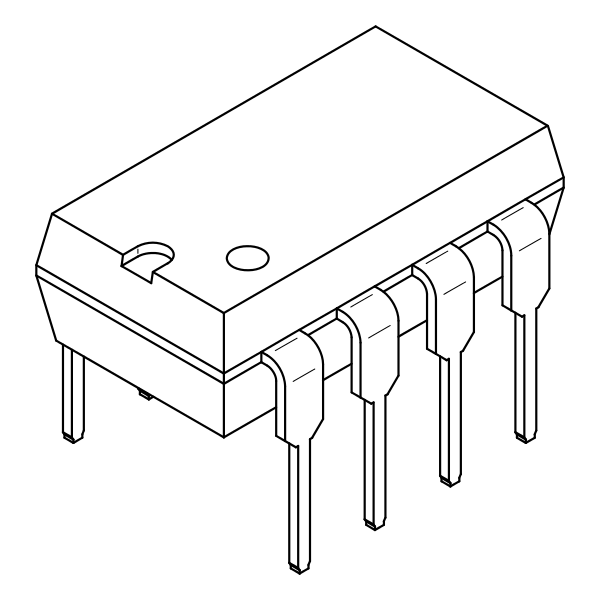
Through-hole packages are a type of integrated circuit (IC) package that are typically used in older electronics and in applications where reliability is a key concern. Unlike surface-mount packages, which are soldered to the surface of a printed circuit board (PCB), through-hole packages have leads that are inserted into holes in the PCB. Here are some of the most common types of through-hole packages, along with their key features:
| Package Name | Description | Advantages | Disadvantages |
|---|---|---|---|
| Dual In-Line Package (DIP) | This package features two parallel rows of pins that are inserted into holes on a PCB. | Versatile and available in a range of sizes and pin counts. Easy to handle and less prone to damage compared to surface-mount packages. | Large size makes them less suitable for high-density applications where space is limited. |
| Plastic Leadless Chip Carrier (PLCC) | This package features leads that wrap around the perimeter of the package and are soldered to the PCB. | Provides a strong mechanical connection to the PCB, making it ideal for applications where a robust and reliable connection is required. | More complex to manufacture compared to other types of packages. |
| Flat Package (FP) | This package features leads that are arranged in a single row and inserted into holes on a PCB. | Simple and easy to handle. Available in a range of sizes and pin counts. | Limited number of connections compared to other types of packages, making it less suitable for high-performance applications. |
In conclusion, through-hole packages are still widely used in many applications where reliability and robustness are key design considerations. However, as technology advances and the demand for high-density and high-performance applications grows, surface-mount packages have become increasingly popular due to their smaller size, higher pin density, and ease of PCB manufacturing.

Surface-mount packages are a type of integrated circuit (IC) package that are designed for use in modern electronics. Unlike through-hole packages, which have leads that are inserted into holes in a printed circuit board (PCB), surface-mount packages are soldered directly to the surface of a PCB. This allows for higher density and higher performance compared to through-hole packages. Here are some of the most common types of surface-mount packages, along with their key features:
| Package Name | Description | Advantages | Disadvantages |
|---|---|---|---|
| Quad Flat Package (QFP) | This package features leads arranged in multiple rows around the perimeter of the package and soldered to the surface of the PCB. | High pin density and versatility, making it suitable for a wide range of applications. | Requires specialized equipment and processes to manufacture and assemble. |
| Ball Grid Array (BGA) | This package features a array of small solder balls on the bottom surface that are soldered to the surface of the PCB. | High pin density, allowing for more connections and higher performance compared to other types of packages. | Complex to manufacture and challenging to repair if damaged. |
| Small Outline Integrated Circuit (SOIC) | This package features leads that are arranged in two parallel rows and soldered to the surface of the PCB. | Small size, making it suitable for high-density applications where space is limited. | Limited number of connections compared to other types of packages, making it less suitable for high-performance applications. |
In conclusion, surface-mount packages have become the dominant technology for modern electronics due to their smaller size, higher pin density, and ease of manufacturing. However, their complexity and difficulty in repair means that they are less suited for applications where reliability and robustness are key design considerations. Through-hole packages are still used in these applications due to their greater reliability, but they are becoming increasingly rare as surface-mount technology continues to evolve and improve.

Pin Grid Array (PGA) is a type of integrated circuit (IC) package that features a grid of pins that are soldered to a printed circuit board (PCB). PGA packages are used in a variety of applications, including microprocessors, memory modules, and other high-performance electronics. Here are some of the most common types of PGA packages, along with their key features:
| Package Name | Description | Advantages | Disadvantages |
|---|---|---|---|
| Disadvantages | This package features a grid of pins that are arranged in a square or rectangular pattern and soldered to the surface of a PCB. | High pin density, allowing for more connections and higher performance compared to other types of packages. | Prone to damage during handling and assembly, and can be difficult to repair if damaged. |
| Ceramic Pin Grid Array (CPGA) | This package features a grid of pins that are arranged in a square or rectangular pattern and soldered to the surface of a PCB. The package itself is made of ceramic material. | Offers improved thermal performance compared to plastic PGA packages, making it suitable for high-performance applications. | More expensive to manufacture and assemble compared to plastic PGA packages. |
In conclusion, PGA packages are widely used in high-performance applications due to their high pin density and versatility. However, the difficulty of handling and repairing PGA packages means that they are less suitable for applications where reliability and robustness are key design considerations. In these applications, other types of packages, such as through-hole packages or surface-mount packages, may be more appropriate.
IC packages play a critical role in the design and performance of modern electronics. They provide protection, improved reliability, and space-saving benefits, but also come with added costs and limitations. To better understand their impact on the design and performance of electronic devices, we need to know the advantages and disadvantages of IC packages.
The advantages of IC packages include protection for sensitive components, improved reliability, space-saving, ease of assembly, and improved performance. By providing protection from physical damage, moisture, dust, and other environmental factors, the life span of the device is extended, and its reliability is improved. IC packages are also much smaller in size compared to individual components, allowing for compact designs and increased density of components on a circuit board. This compact size also makes assembly easier and more cost-effective. In addition, IC packages can also improve performance by reducing noise and providing better thermal management.
| Advantages | Explanation |
|---|---|
| Explanation | IC packages provide protection to the sensitive components within from physical damage, moisture, dust and other environmental factors. |
| Improved Reliability | By encapsulating the delicate electronics within a protective package, the reliability of the device is improved and its life span is extended. |
| Space-saving | IC packages are much smaller in size compared to individual components, allowing for compact designs and increased density of components on a circuit board. |
| Ease of Assembly | Packaging allows for easy and automated assembly of components, reducing manufacturing costs. |
| Improved Performance | IC packages can also improve performance by reducing noise and providing better thermal management. |
| Advantages | Explanation |
|---|---|
| Cost | IC packages can be more expensive than individual components and add to the cost of the device. |
| Complexity | Some IC packages are complex and may require specialized equipment and technical expertise for assembly and repair. |
| Limited Repairability | If a component within the package fails, it may be difficult or impossible to repair without replacing the entire package. |
| Package Dependent Characteristics | The performance of the device may be dependent on the package, and changing the package may alter the device's behavior. |
| Thermal Management | Some IC packages may not provide adequate thermal management, leading to overheating and reduced performance or reliability. |
The essential elements of an IC package are its size, shape, and material composition. The size of the package should be appropriate for the type and size of the component being used, and the shape of the package should allow for easy installation and removal. The material composition of the package should be appropriate for the application and should be able to withstand the environmental conditions of the application.
The most common methods of IC package I/O termination include peripheral, grid-array, ball-grid array, and flip-chip. Peripheral I/O termination involves the placement of terminals around the edges of the chip or package, while grid-array I/O termination involves the placement of terminals on the bottom surface of the chip or package. Ball-grid array I/O termination involves the placement of terminals on the bottom surface of the chip or package, and are in the form of solder spheres. Flip-chip I/O termination involves the placement of terminals on the top surface of the chip. The terminal pitch is the distance between the terminal pins or pads, which can vary from 0.025”to 0.100”or more.
When selecting an IC package, it is important to research the requirements of the application and the type of component to be used. The size, shape, and material composition of the package should be appropriate for the application, and the type of package should be selected based on its cost-effectiveness and reliability. Also, it is important to use the appropriate level of protection for the application, such as a conformal coating or a moisture barrier bag.
In summary, IC packages are an essential component of many electronic devices. There are several different types of IC packages, each of which has its own advantages and disadvantages. The essential elements of an IC package are its size, shape, and material composition, and it is important to select the appropriate package for the application. Finally, the best practices for selecting and using IC packages include researching the requirements and understanding the different types of packages, as well as using the appropriate level of protection.
Still, need help? Contact Us: support@nextpcb.com
Need a PCB or PCBA quote? Quote now


 Surface

