NextPCB Capabilities
Printed Circuit Boards
NextPCB Capabilities
Printed Circuit Boards
 PCB Assembly
 Layer Buildup
 SMD-Stencils
 PCB Design-Aid & Layout
 Mechanics
 Quality
 Drills & Throughplating
 Factory & Certificate
 PCB Assembly Factory Show
Certificate
PCB Assembly Factory Show
Certificate
Support Team
Feedback:
support@nextpcb.com


Time to send your design off for manufacture, but the engineers are asking for a pick and place file? In this guide, we cover what a pick and place (centroid) file is, how to export it from KiCad, and what the configuration options mean. Whether you are preparing files for JLCPCB, PCBWay, NextPCB or your own assembly setup, this guide tells you everything you need to know.
The pick and place file is a machine-readable document that tells automated assembly equipment the location and rotation of surface-mount devices (SMD) that go onto a PCB board. Equipment like the pick and place machine uses this to “know” where and how to place the parts on the bare PCB board.
The pick and place file may also be referred to as the PnP file (P&P), xy file, centroid file, footprint position file, etc. In KiCad, it is called the Component Placement File (previously Footprint Position File) and has the default file extension of .pos, which stands for position.
The export process is very straightforward if your assembly house is flexible with file formats. In fact, the biggest hurdle was probably knowing it is called a Component Placement file and not pick and place or Centroid file.
The following instructions were made for KiCad 9; however, the process has largely remained unchanged - at least since KiCad 6, with only minor changes to the export options. We’ll cover the KiCad 6 options in this article as well.
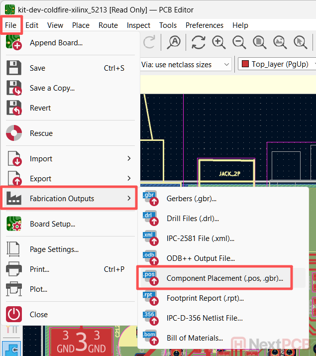
In KiCad, open your design in the PCB editor and go to File -> Fabrication Outputs -> Component Placement File (.pos, .gbr)...
In the new window called Generate Placement Files, fill in the Output directory.
If your manufacturer is flexible in terms of format or has not specified requirements, the default options most likely will suffice. However, we will go through the meaning and impact for each option in the next section.
Then click Generate Position File and verify the export was successful in the Output Messages box.
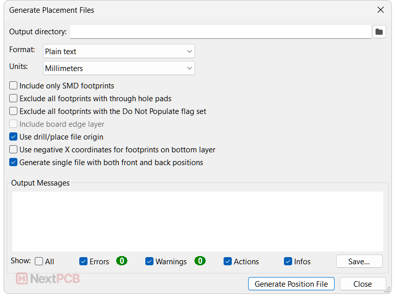
In KiCad 6, the options are very similar just laid out differently with some exceptions. ASCII refers to Plain Text format in KiCad 9 and there is no option to exclude Do Not Populate parts and use negative coordinates for the bottom layer.
First things first, you should always follow your assembly house’s recommendations if available. Although many modern machines can accept a variety of formats, some older machines and specific circumstances may require different settings. You should always follow the instructions of the party doing your assembly, first and foremost.
Below you can see the differences between the Plain Text or ASCII export and the CSV format export when opened in a text editor. Technically, they are both in ASCII text files, which is probably why the option was changed to Plain Text in later KiCad versions.
The plain text export has the file extension .pos, while the csv version has the suffix .csv.
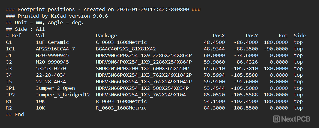
Plain text/ASCII KiCad pick and place output
As you can see, the Plain Text version is very human-readable, is neatly arranged in columns, and comes with some extra export information in the header. It’s not very spreadsheet-friendly, however, and may require a few more steps if you need to make modifications in a spreadsheet program.
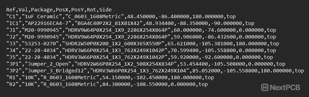
CSV (comma-separate values) KiCad pick and place output
The CSV export, on the other hand, can use the semicolon as the delimiter and quotation marks as the text qualifier to cleanly separate the columns. This is important if you need to modify the file for compatibility with highly automated services like JLCPCB, for example.
For the units, choose whichever you prefer or is required by your assembly house.
Traditionally, the pick and place file only contained surface mount parts (SMD) since, back in the day, these were the only parts that would be placed by pick and place machines. Through-hole components were largely inserted by hand.
This is no longer necessarily the case, and it can be beneficial to include through-hole parts in the centroid file, even if it is not used by the SMD soldering process.
The software HQDFM, for example, needs the position information of THT parts to perform DFM analysis (for clearances, etc.). It is simply a way to tell machines the position and rotation of a part.
Again, this largely depends on the preference of your manufacturer; however, this is the one default setting I would advise changing.
Combining the top and bottom files does not eliminate data, but simply adds another column containing side information. This can be understood by many modern software, and I would say it is the more modern, smart approach. In fact, many software and portals only allow you to upload one pick and place file. For example, many online quotation forms, and even the HQDFM DFM software expects a single file.
Eagle-eyed users may have noticed Gerber X3 in the list of format options. X3 differs from RS-274x and X2 Gerber formats in that it is not a Gerber file format per se, but an additional Gerber file containing assembly attributes, including component placement information. It is a Gerber 2D-graphical image format; however, not a simple ASCII list, which allows you to visualize the data just as you would view the Gerber files.
Thus, as a graphical format, choosing Gerber X3 format activates the Include board edge layer option. Including this can act as a guide for human inspection. You can even print it out 1:1 to match the board exactly. Kind of like a silkscreen layer.
But before we get ahead of ourselves, unfortunately, the new X3 format has not caught on well with software developers and manufacturers. In fact, I can’t think of one mainstream manufacturer that accepts it. Perhaps this will change in the near future.
Choosing Gerber X3 export outputs a .gbr file per side, and looks like this in a Gerber viewer (HQDFM):
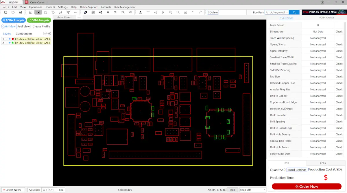
KiCad Gerber X3 files opened in HQDFM. You need a CAD system that supports X3 to be able to ‘see’ the X3 attributes in CAM view.
With their highly automated ordering system, getting the CPL file through their system first time can be a pain. As per their own instructions, the pick-and-place file needs to be edited to be compatible with their online ordering system. The file exported from KiCad will not work as is.
According to the website, the following settings are required:
Format: CSV only
Units: Millimeters
Headers required: Designator, Mid X, Mid Y, Rotation and layer
After exporting your component placement file from KiCad, import it into a spreadsheet program or text editor and change the headers to match JLCPCB’s requirements.
| KiCad Header | JLCPCB Header |
|---|---|
| Ref | Designator |
| PosX | Mid X |
| PosY | Mid Y |
| Rot | Rotation |
| Side | Layer |
We tested this with a file exported from KiCad 9, and it seems only the PosX and PosY headers need changing. If you need to modify the values, for example, to fix rotation issues, import them into spreadsheet software like Excel, WPS, or OpenOffice and edit them there.
PCBWay's assembly service is largely 'offline', that is, no parsing of the assembly and pick and place files is performed. The good thing about this is that it generally means the engineers are more flexible in terms of format. So feel free to use the default settings outlined above to export the files.
Similarly, NextPCB's PCBA requirements are very laid back. We like to call it the centoid file, and we accept CSV and plain text pick-and-place files in virtually any configuration. Since engineers perform DFA review for every order (after order confirmation and during assembly setup), any discrepancies in the centroid file will be highlighted or corrected by cross-referencing the available data.
HQDFM is a PCB design analysis suite with DFM and DFA capabilities developed by NextPCB. For Design for Assembly (DFA) review, the pick and place (centroid file) is required with the following settings:
File format: CSV is recommended
Units: Any
Headers required: Supports auto-matching and manual assignment of headers
Do not check the Include only SMD footprints option.
Check the Generate single file with both front and back positions option.
Other options can be left to their default values.
HQDFM maps components onto the Gerber visualization using the centroid file. It then uses its internal library of over 6 million parts to import footprint, size, and shape data for a complete Design for Assembly (DFA) analysis, identifying overlapping components, incorrect pad sizes, clearances, overhanging parts, etc. There is also a graphical interface for editing pick and place files manually, which is useful for moving through-hole component positions that have the centroid origin on pin 1 rather than the component center.
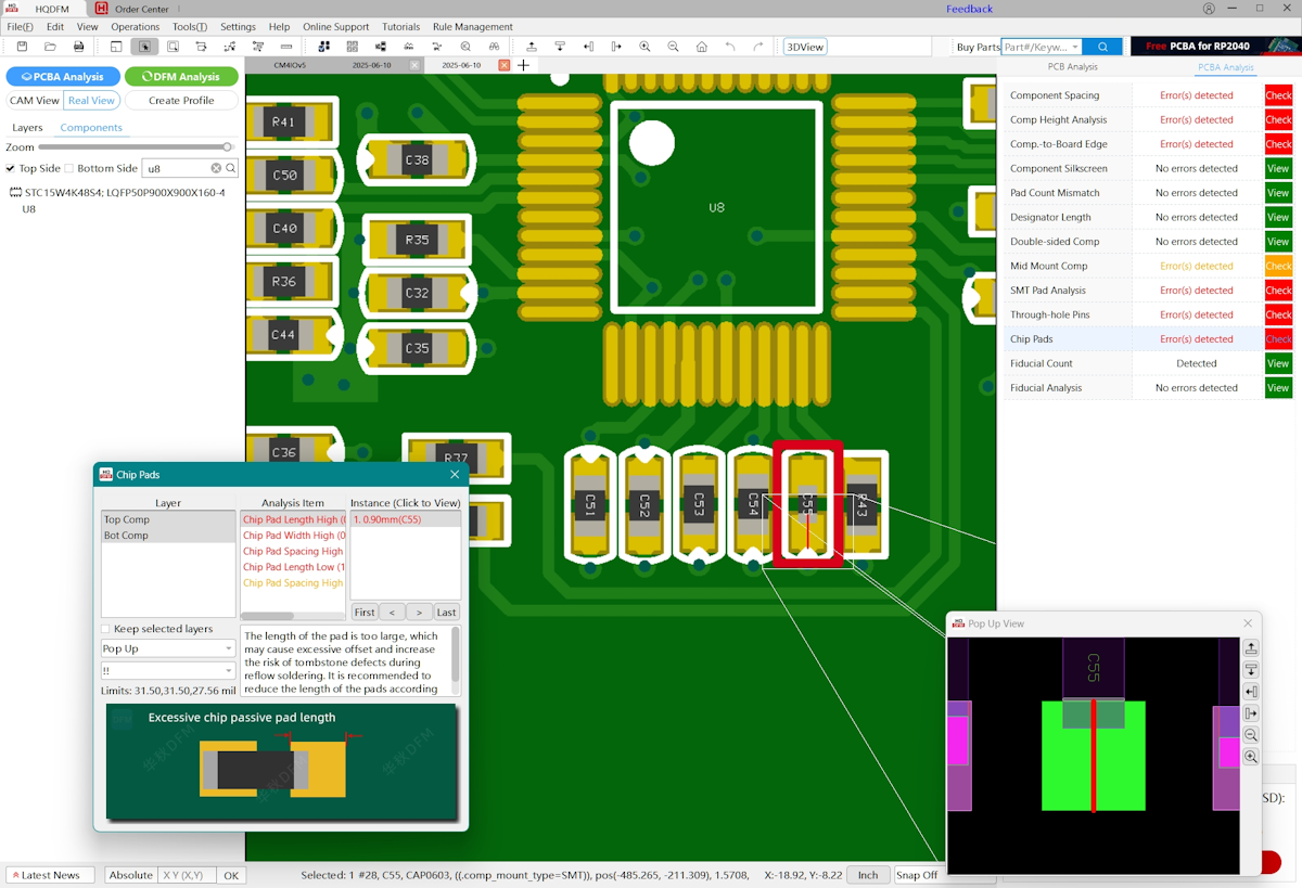
PCB Design for Assembly (DFA) in HQDFM
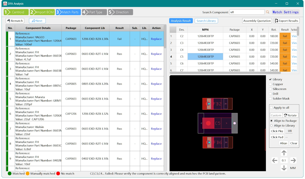
Pick and place file graphical editor in HQDFM
If one or both of your pick and place files are empty, it could just be that your design does not have any surface mount components! Traditionally, pick and place files only contained location data for surface mount components, since through hole components were, and still are, largely inserted by hand in non-mass production settings. Eventually, location data for all components on the board became useful for other means, (design analysis software for example) and so more and more software allow the location of through-hole components to be exported as well. So, if your design consists of only through-hole components, (and you select to Include only SMD footprints or Exclude all footprints with through-hole pads) the pick and place files will be pretty empty.
If only a few components are missing, check if these components have through-hole pads. The option Exclude all footprints with through hole pads differs from the Include only SMD footprints option in that any part, even if it is considered surface mount and has surface-mount pads, will be excluded if it has a through-hole pads (think USB ports).
Another thing to check is if the missing parts are marked as Do Not Populate (DNP) in the schematic editor, and the Exclude all footprints with the Do Not Populate flag set checkbox is selected.
HQDFM is a free PCB design analysis suite for analysis PCB production files including Gerber, ODB++, BOM and Centroid (pick-and-place) files. One of it's most powerful features is Design for Assembly (DFA) review, which detects assembly-related errors and potential pitfalls just from the production files.
The wizard-guided workflow includes a pick and place verification stage that cross-references centroid data with the BOM and Gerber data/ODB++ data. It uses this to identify inconsistencies, duplicates, and even allows editing of individual pick-and-place data in a graphical interface, great if you need to make individual tweaks or change the rotation. If your pick and place data has errors, most likely, HQDFM can detect them. Click here to download.
An important thing to note is that the rotation shown in your EDA tool has no relationship to how the component is oriented in its manufacturer‑supplied packaging (tape, reel, tray, or tube). There is no universal convention for packaging orientation, so the rotation in your pick‑and‑place file will almost never match the rotation of the part as it arrives at the assembly house.
Because of this, the pick‑and‑place file should be treated as the definition of how the component is intended to sit on the PCB — not how it sits in the reel. Silkscreen pin‑1 markers, polarity indicators, and asymmetric outlines should always be clear and consistent to reinforce the correct orientation for polarized and directional components.
Once the assembly house understands the intended PCB orientation, they apply their own rotation correction based on how the component is fed into the machine. This ensures the part is placed correctly regardless of its packaging orientation.


NextPCB provides PCB manufacturing and assembly services, focusing on reliability without breaking the bank. With 5 factories in China and over a decade of quick turnaround electronics manufacturing from prototype to mass production, NextPCB serves over 160 countries around the world, pairing dependable electronics hardware with exceptional service.
As a Platinum KiCad sponsor and long-term supporter of the KiCad open-source ecosystem, NextPCB's contribution spans developer funding, and hosting KiCon Asia — the largest KiCad‑focused event in the region. This KiCad Hub brings together all of our tutorials, tools, projects, and community contributions into one place, making it easier for designers of all levels to learn, explore, and build with KiCad.
Still, need help? Contact Us: support@nextpcb.com
Need a PCB or PCBA quote? Quote now


 Surface