
 NextPCB Capabilities
Printed Circuit Boards
NextPCB Capabilities
Printed Circuit Boards
 PCB Assembly
 Layer Buildup
 SMD-Stencils
 PCB Design-Aid & Layout
 Mechanics
 Quality
 Drills & Throughplating
 Factory & Certificate
 PCB Assembly Factory Show
Certificate
PCB Assembly Factory Show
Certificate
Support Team
Feedback:
support@nextpcb.com


In modern electronic design, with the proliferation of high-speed digital circuits (such as DDR, PCIe) and the rapid increase in component integration, traditional 4-layer boards often struggle to provide complete signal return paths or meet increasingly strict Electromagnetic Compatibility (EMC) requirements. Consequently, 6-layer boards have become a standard choice for many mid-to-high-end industrial control, consumer electronics, and communication products. Compared to 4-layer boards, 6-layer designs not only provide additional routing space but, more importantly, enable a superior reference plane layout to suppress inter-layer crosstalk and electromagnetic radiation at the physical structural level.
This article explores the underlying logic of layer arrangement through several classic 6-layer structures and uses a NextPCB-recommended 6-layer HDI (High-Density Interconnect) stackup impedance solution as an example to discuss how hardware engineers can select a reasonable stackup that balances Signal Integrity (SI) and Design for Manufacturing (DFM). >> View More Common HDI Stackup Types (1+N+1, 2+N+2 and More)
Conventional 6-layer through-hole board stackups have various combinations. When evaluating these structures, engineers typically use two core criteria: first, whether signals have adjacent and continuous reference planes (providing the shortest return path); and second, whether a significant planar capacitance can be formed between the power and ground planes (reducing high-frequency power impedance).
| Layer | Structure 1 | Structure 2 | Structure 3 |
|---|---|---|---|
| Layer 1 (Top) | Signal Layer (Components, Microstrip) | Signal Layer (Components, Microstrip) | Signal Layer (Components, Microstrip) |
| Layer 2 | Signal Layer (Embedded Microstrip) | Ground Plane | Power Plane |
| Layer 3 | Ground Plane | Signal Layer (Stripline) | Ground Plane |
| Layer 4 | Power Plane | Signal Layer (Stripline) | Signal Layer (Stripline) |
| Layer 5 | Signal Layer (Embedded Microstrip) | Power Plane | Ground Plane |
| Layer 6 (Bottom) | Signal Layer (Components, Microstrip) | Signal Layer (Components, Microstrip) | Signal Layer (Components, Microstrip) |
In this structure (typically arranged as SIG-GND-SIG-SIG-PWR-SIG), the Top and Bottom layers serve as surface routing layers, with two internal routing layers and two reference planes.
This structure (e.g., SIG-PWR-SIG-SIG-GND-SIG) also provides four routing layers but pushes the power and ground planes to Layer 2 and Layer 5, respectively, with two internal signal layers sandwiched between them.
When system Signal Integrity requirements are extremely high and three signal layers are sufficient for all network connections (e.g., SIG-GND-PWR-SIG-GND-SIG), this is a very stable design with excellent shielding.
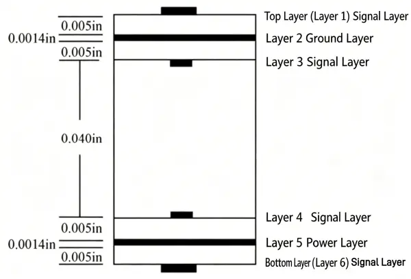
Example of Traditional Asymmetrical Impedance Design:
In certain manufacturing scenarios, the dielectric thicknesses of a 6-layer board might be unequal. For instance: Top Layer (1oz copper, horizontal routing, 8mil width / 25mil spacing) controls 50Ω single-ended impedance; Layer 2 is a continuous ground plane; Layer 3 (1oz copper, vertical routing, using a 6.5mil width / 25mil spacing offset stripline design due to different distances from upper and lower reference planes) controls 50Ω impedance; Layer 4 is the same as Layer 3 but with horizontal routing; Layer 5 is the power plane; and the Bottom Layer (also 8mil width) controls 50Ω impedance.
As chip manufacturing processes evolve, BGA component pitch continues to shrink (e.g., 0.65mm, 0.5mm, or even smaller). In such high-density scenarios, traditional Plated Through-Hole (PTH) processes often face physical limits in hole size and pad diameter, making it impossible to fan out signals from the center of a BGA via "Dog-bone" patterns. In these cases, adopting a 1+4+1 HDI structure with laser-drilled blind and buried vias becomes a practical choice to break through physical space bottlenecks.
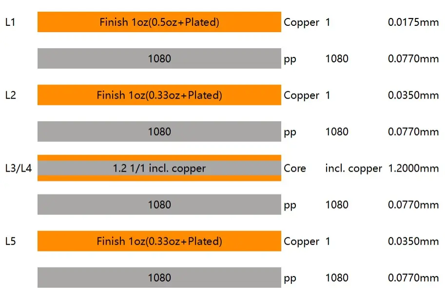
Let's look at how stackup data is implemented in a real factory process, based on the 6-layer HDI board stackup impedance solution recommended by NextPCB.
The so-called "1+4+1" refers to a micro-via structure containing one layer of blind vias on each outer side (L1-L2, L6-L5) and a four-layer core in the middle (containing L2-L5 mechanical buried vias). Below are typical parameters from a real production line:
| Layer/Material | Layer Property | Copper Thickness (Finished) | Dielectric Thickness (mm) | Remarks / Via Structure |
|---|---|---|---|---|
| L1 | Top Signal | 1 oz | - | Surface signal layer, fanned out via L1-L2 laser blind vias |
| Prepreg | PP (1080) | - | 0.076 | Thin dielectric layer suitable for laser drilling |
| L2 | GND | 1 oz | - | Reference ground plane, containing L2-L5 mechanical buried vias |
| Core | FR-4 (Dk ~4.2) | - | 0.1 / 0.8 | Core thickness adjusted based on total board thickness |
| L3 | Signal / PWR | 1 oz | - | Internal signal or power plane layer |
| Prepreg | PP (2116) | - | 0.11 | Conventional prepreg |
| L4 | Signal / PWR | 1 oz | - | Internal signal or power plane layer |
| Core | FR-4 (Dk ~4.2) | - | 0.1 / 0.8 | Core thickness adjusted based on total board thickness |
| L5 | GND | 1 oz | - | Reference ground plane |
| Prepreg | PP (1080) | - | 0.076 | Thin dielectric layer suitable for laser drilling |
| L6 | Bottom Signal | 1 oz | - | Surface signal layer, fanned out via L6-L5 laser blind vias |
(Note: Specific Core and PP models are flexibly adjusted based on the customer's final target board thickness, such as 1.0mm or 1.6mm.)
In this solution, HDI technology brings not only a reduction in via footprint but also inevitably involves thinner outer dielectrics (e.g., 0.076mm thick 1080 PP to accommodate laser drilling). This physical change has a direct and significant impact on impedance control:
Engineer's Troubleshooting Guide (Impedance Deviation Traps): In the early stages of design, many engineers rely on internal EDA tools (like those in Altium or Cadence) or third-party simplified tools to calculate impedance. However, theoretical values often ignore the actual factory resin flow rate during pressing, the etching factor (traces are trapezoidal rather than rectangular), and the dielectric constant impact of the solder mask thickness, leading to out-of-tolerance impedance after prototyping.
To ensure consistency between simulation and actual measurement, it is highly recommended to use real empirical data calibrated by the factory's production lines. You can visit the NextPCB Impedance Calculator and Stackup Recommendation Tool (https://www.nextpcb.com/pcb-impedance-calculator) at the start of your design to select a lamination structure that matches manufacturing reality, eliminating SI risks at the source.
>>> Read more: Comparison of 4-layer PCB Stack-ups
Determining the stackup, calculating impedance, and completing the laborious routing does not mean the design is foolproof. There is often a "process gap" between theoretical design and actual manufacturing. For example: does the 4mil trace width calculated for impedance meet the minimum etching capability for the chosen copper thickness? Is the internal copper pour too close to the drill holes, risking a short circuit?
To avoid time and financial costs wasted on prototype rework, it is recommended that engineers use automated DFM (Design for Manufacturing) analysis software to perform comprehensive inspections after outputting Gerber files. You can try the HQDFM tool (https://www.nextpcb.com/dfm). This tool can analyze potential manufacturing hazards—such as acute angle traces (acid traps), open/short circuit risks, excessive drill aspect ratios, and impedance trace width/spacing compliance—based directly on actual factory process capabilities with a single click.
Excellent 6-layer board design is not just about stacking layers or connecting networks; it is a systematic trade-off between return paths, power integrity, and manufacturing process limits. When space allows and cost sensitivity is high for conventional designs, reasonably arranging reference planes (as in Configuration 3) is a great low-cost way to improve signal quality. In the face of high-density BGAs and space-constrained portable devices, adopting a mature HDI 1+4+1 standard stackup as provided by NextPCB, complemented by rigorous HQDFM pre-manufacturing checks, is a pragmatic choice that balances electrical performance with mass-production reliability.
| Check NextPCB's Standard 6-Layer Stackup Configurations |
Before finalizing your 6-layer stackup in your EDA tool, verify that your chosen prepreg and core combination is available in production. NextPCB's stackup tool shows real manufacturing options with impedance values for each configuration.
Q: What is the maximum acceptable dimple size for Via-in-Pad microvias?
A: According to IPC-6012 standards, the maximum allowable dimple (indentation) depth for VIPPO (Via-in-Pad Plated Over) should not exceed 15μm. Exceeding this limit significantly increases the risk of solder voids during BGA assembly. It is highly recommended to require a Microsection Report in your Fab Notes to verify these parameters.
Q: Why do microvias frequently fail during reflow soldering in a 1-4-1 HDI PCB?
A: This is typically caused by Z-axis CTE (Coefficient of Thermal Expansion) mismatch. At reflow temperatures (up to 260°C), the expansion force can cause interfacial fracture where the laser microvia separates from the target pad. This is often exacerbated by moisture absorption or improper resin filling in the underlying buried vias.
Q: Is a 2-N-2 (2-2-2) structure better than a 1-N-1 (1-4-1) for a 6-layer HDI PCB?
A: The choice depends on a trade-off between interconnect density and cost. A 1-4-1 structure is more economical as it requires only one build-up cycle. A 2-2-2 structure supports stacked vias for complex fan-outs but involves two build-up cycles, which increases costs and subjects the board to more thermal stress during fabrication.
Still, need help? Contact Us: support@nextpcb.com
Need a PCB or PCBA quote? Quote now


 Surface

