
 NextPCB Capabilities
Printed Circuit Boards
NextPCB Capabilities
Printed Circuit Boards
 PCB Assembly
 Layer Buildup
 SMD-Stencils
 PCB Design-Aid & Layout
 Mechanics
 Quality
 Drills & Throughplating
 Factory & Certificate
 PCB Assembly Factory Show
Certificate
PCB Assembly Factory Show
Certificate

Support Team
Feedback:
support@nextpcb.com


As modern electronic systems become faster and more complex, PCB designers must address challenges related to signal integrity, electromagnetic interference (EMI), and power stability. High-speed interfaces such as DDR, USB, PCIe, and high-frequency microcontrollers generate rapid switching signals that require carefully designed PCBs to ensure reliable operation and minimal noise.

Illustration of a 4-layer PCB stackup highlighting signal layers, ground plane, and power plane for high-speed digital circuits
One effective way to improve performance is by using a 4-layer PCB instead of a traditional 2-layer board. Multilayer PCBs allow designers to dedicate internal layers for ground and power planes, improving signal return paths, reducing EMI, and enabling controlled impedance routing. In this article, we explore how to design an effective 4-layer PCB stackup for high-speed digital circuits, including layer configuration, materials, and practical design guidelines.
A PCB stackup refers to the arrangement and order of conductive copper layers and insulating dielectric materials that make up a printed circuit board. It defines how signal layers, power planes and ground planes are organized vertically inside the PCB.
In multilayer boards, the stackup determines several critical electrical properties, including signal integrity, impedance control, and electromagnetic compatibility. Because high-speed digital signals behave more like electromagnetic waves than simple electrical connections, the physical structure of the PCB plays a major role in how these signals propagate.
A typical PCB stackup consists of the following elements:
While 2-layer PCBs are suitable for simple circuits, they often struggle with signal integrity, EMI, and power stability in high-speed designs. A 4-layer PCB addresses these issues by introducing dedicated ground and power planes, which provide low-impedance return paths and enable controlled impedance routing.
With a continuous ground plane and internal shielding, 4-layer boards offer better signal integrity, reduced EMI, improved power distribution, and easier routing. This makes them ideal for modern high-speed applications such as processors, FPGAs, and communication systems.
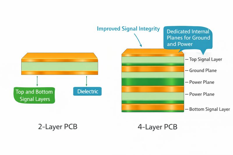
Comparison of 2-layer and 4-layer PCBs showing how additional layers improve signal integrity and power distribution
The differences between 2-layer and 4-layer PCBs become clearer when comparing their capabilities.
| Feature | 2-Layer PCB | 4-Layer PCB |
|---|---|---|
| Signal Integrity | Limited | Much better due to ground plane |
| EMI Control | Weak | Improved shielding |
| Power Distribution | Routed traces | Dedicated power plane |
| Routing Flexibility | Limited | Higher |
| Suitability for High-Speed | Poor | Ideal for moderate high-speed designs |
Because of these advantages, 4-layer PCBs are widely used in embedded systems, communication devices, industrial controllers, and high-speed digital electronics.
A well-designed stackup is essential for maintaining signal integrity in high-speed PCBs. The most commonly used 4-layer configuration provides an optimal balance between performance, EMI control, and manufacturability.
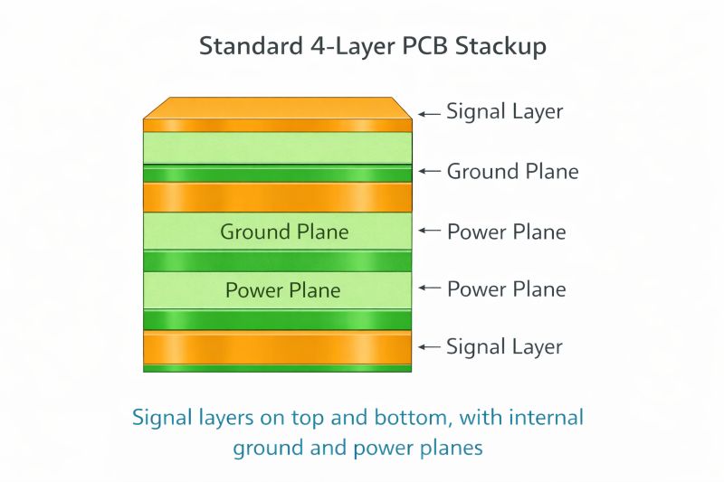
Standard 4-layer PCB stackup configuration with signal layers on top and bottom and internal ground and power planes
The standard structure consists of four copper layers:
In this arrangement, the outer layers are used for signal routing, while the inner layers are dedicated to solid ground and power planes. The ground plane provides a low-impedance return path for high-speed signals, helping to reduce noise and maintain signal integrity.
The close coupling between the ground and power planes improves power stability and reduces electromagnetic interference (EMI). This structure also simplifies routing by separating signal and power distribution, making it ideal for most high-speed digital designs.
Because of its simplicity and strong electrical performance, this stackup is widely used in embedded systems, communication devices, and modern high-speed electronic circuits.
Although the standard Signal–Ground–Power–Signal configuration works well for many designs, different applications may require alternative stackup arrangements. The optimal stackup depends on factors such as signal speed, EMI requirements, power distribution complexity, and routing density.
Below are some commonly used alternative 4-layer stackup configurations.
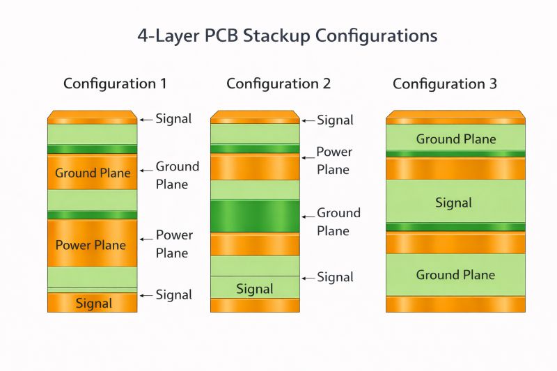
Common 4-layer PCB stackup configurations used for different signal integrity and EMI requirements
Option 1: Signal – Power – Ground – Signal
This configuration places the power and ground planes adjacent to each other in the center of the PCB. The close coupling between the power and ground layers creates strong inter-plane capacitance, which helps stabilize the power distribution network.
However, because the top signal layer references a power plane instead of a ground plane, signal integrity may not be as strong as in the standard configuration. Designers often use this stackup in boards where power stability is more critical than extremely high-speed signal routing.
Option 2: Ground – Signal – Signal – Ground
This stackup sandwiches the signal layers between two ground planes, providing excellent shielding and EMI performance. The ground planes act as protective layers that contain electromagnetic radiation generated by high-speed signals.
This configuration is sometimes used in RF designs, sensitive analog circuits, or systems with strict EMI requirements. However, it may reduce routing flexibility because the outer layers are dedicated to ground.
Option 3: Signal – Ground – Signal – Power
This arrangement allows designers to route signals on two internal layers while keeping a solid ground reference close to critical traces. It is sometimes used in designs that require additional routing space while still maintaining a nearby ground reference.
The electrical performance of a PCB stackup is not determined only by the layer arrangement; the dielectric materials and thickness between layers also play a major role. These parameters influence impedance, signal propagation speed, and overall board reliability.
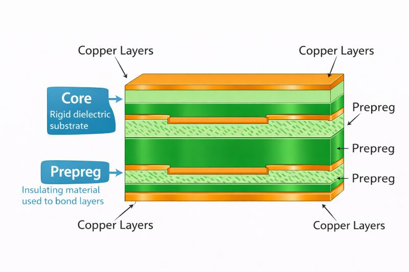
PCB internal structure illustrating core and prepreg materials used to bond copper layers
Most standard PCBs use FR-4, a glass-fiber reinforced epoxy laminate. FR-4 is widely used because it offers a good balance of electrical performance, mechanical strength, and cost.
However, in very high-speed or high-frequency designs, specialized materials such as Rogers laminates or high-performance FR-4 variants may be used. These materials provide more stable dielectric properties and lower signal loss at high frequencies.
In multilayer PCBs, dielectric layers typically consist of two types of materials:
The combination of core and prepreg layers determines the distance between copper planes, which directly affects impedance and signal coupling.
Typical 4-Layer PCB Stackup Thickness Example
| Layer | Type | Typical Thickness |
|---|---|---|
| Layer 1 | Signal | 35 µm copper |
| Dielectric | Prepreg | 0.18 mm |
| Layer 2 | Ground Plane | 35 µm copper |
| Dielectric | Core | 0.8 mm |
| Layer 3 | Power Plane | 35 µm copper |
| Dielectric | Prepreg | 0.18 mm |
| Layer 4 | Signal | 35 µm copper |
Dielectric thickness directly affects trace impedance by controlling the distance between a signal layer and its reference plane; thinner dielectric reduces the required trace width for a target impedance (e.g., 50 Ω) and improves signal control. It also influences signal coupling, noise performance, and power-plane capacitance, making it a key factor in high-speed PCB design, so designers typically follow manufacturer-recommended stackups to ensure accurate impedance and reliable performance.
In high-speed digital circuits, signal traces must often maintain a specific impedance to ensure proper signal transmission. When impedance is not controlled, signals can experience reflections, distortion, and timing errors, which may lead to communication failures in high-speed interfaces.
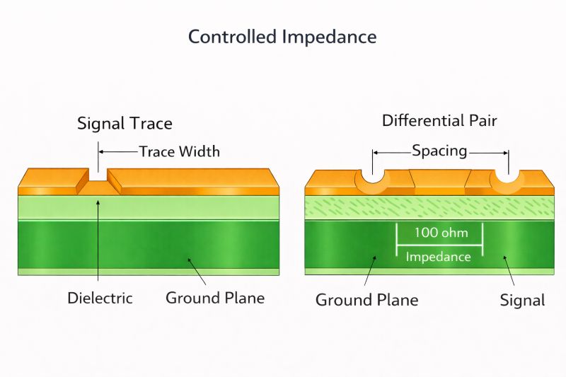
Controlled impedance routing in PCB design showing trace width, dielectric spacing, and differential pair configuration
Controlled impedance is particularly important for interfaces such as USB, HDMI, PCIe, DDR memory, Ethernet, and high-speed serial communication. These signals typically require a defined impedance value to maintain signal integrity across the PCB.
Two common impedance types used in PCB design are:
Single-ended signals are referenced to a ground plane and typically require 50 Ω impedance. These are commonly used for clock lines, control signals, and certain communication interfaces.
Differential signals consist of two complementary traces that carry opposite signals. The impedance is defined between the pair of traces and is usually 100 Ω differential for many high-speed protocols.
Maintaining controlled impedance depends on several physical parameters of the PCB:
For example, if the dielectric thickness between a signal layer and ground plane increases, the trace width must also increase to maintain the same impedance value.
Because of these dependencies, impedance control is closely tied to the PCB stackup design. Before routing high-speed traces, designers typically define the stackup and use impedance calculators or simulation tools to determine the appropriate trace dimensions.
Working with the PCB manufacturer to define an impedance-controlled stackup ensures that the fabricated board meets the required electrical characteristics.
Maintaining good signal integrity is critical in high-speed PCB design, as poor routing can cause noise, reflections, and timing issues. Key practices include keeping high-speed traces short, routing signals over a continuous ground plane, and avoiding split ground planes to ensure a stable return path.
Additionally, designers should minimize vias, route differential pairs with consistent spacing, and maintain a continuous return path (often using nearby ground vias). Following these practices helps improve signal quality and overall PCB performance.
Maintaining stable power delivery is critical in high-speed PCB design, as rapid switching in devices like microcontrollers and FPGAs can cause voltage fluctuations and noise. A 4-layer PCB improves power integrity by using dedicated power and ground planes, which provide low-impedance current paths and reduce noise. Placing these planes close together also creates distributed capacitance, helping stabilize the power distribution network.
Role of Decoupling Capacitors
| Mistake | Issue Caused | Best Practice |
|---|---|---|
| Split Ground Planes | Breaks return current path, increases EMI and noise | Use a continuous, solid ground plane |
| No Reference Plane | Causes impedance mismatch and signal reflections | Always route signals over a ground plane |
| Incorrect Layer Arrangement | Leads to poor signal integrity and higher EMI | Keep signal layers adjacent to ground planes |
| Ignoring Impedance Control | Results in signal distortion and data errors | Design traces based on controlled impedance |
| Excessive Vias | Introduces inductance and signal discontinuities | Minimize vias for high-speed signals |
To better understand how the stackup works in practice, consider a typical 4-layer PCB used for a microcontroller or embedded system with moderate high-speed interfaces such as USB, Ethernet, or high-frequency clock signals.
A commonly used stackup structure is shown below:
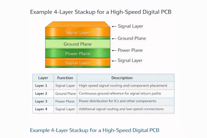
Example of a 4-layer PCB stackup used in high-speed digital circuits with layer functions and descriptions
In conclusion, Designing an effective 4-layer PCB stackup is essential for ensuring reliable performance in high-speed digital circuits, where signal integrity, power stability, and EMI control are critical. By using dedicated ground and power planes, designers can improve return paths, reduce noise, and achieve controlled impedance, while proper layer arrangement minimizes signal reflections and interference. Careful selection of dielectric materials, layer spacing, and routing practices—such as maintaining continuous ground planes, minimizing vias, and placing decoupling capacitors correctly—further enhances performance. For many applications, a 4-layer PCB offers an ideal balance of performance, cost, and manufacturability, though more complex designs may require additional layers. Ultimately, successful PCB design begins with proper stackup planning and close collaboration with manufacturers to ensure both electrical reliability and manufacturability.
Read more: High Quality 4-Layer Printed Circuit Board (PCB) Manufacturing NextPCB
Still, need help? Contact Us: support@nextpcb.com
Need a PCB or PCBA quote? Quote now




