What is a 4 layer PCB?
4 layer PCB suggests there are 4 layers to thrashing electric signals: Leading Layer, Inner Layer 1, Inner Layer 2 as well as Base Layer. TOP, as well as lower layers, are the external layers where we are positioning parts as well as directing. Internal layer 1 as well as internal layer 2 remain in the core and are also generally made use of as power aircraft or utilized for signal routing. As a result, 4 layer PCB = 3 Signal layer + GND layer or 4 layer PCB = 2 signal layers + a VCC layer + a GND layer.
For a 4 layer PCB, why are the power and also ground airplanes typically internal layers, while traces get on the external layers?
Strong power, as well as ground aircraft, are excellent to lower EMI exhausts and also can improve the top quality of the signal on the traces. Furthermore, linking elements to the airplanes is much less complex than to course the power as well as ground trees with traces. The stackup with premises on external layers is claimed to be best from EMC's point of view.
Links in between elements have a tendency to be gathered in your area, as well as those neighborhood links will certainly have a pretty good possibility of being routable on simply one layer. If you place all the traces on the internal layers, you will certainly call for a by means of for all the signals to go from the element to the signal layers.
As an example, when utilizing SMD elements, the links get on the exact same layer as the element, to ensure that there is not require for a by means of or through-hole pad. In space-constrained styles, you have the ability to place even more wiring beyond of the board.
SMT circuity is constantly externally, if your power and also GND were outside, you need to continually break it up for the components being positioned. Besides, it is actually tough to debug, if you place the power as well as GND aircrafts outside of a board. For RF format, the guidelines are various for a trace on the external layer of a board than on the internal layers of a board. It is feasible to make use of less layers if you're doing microstrip directing.
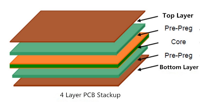
Standard 4 layer PCB stack-up
The standard 4-layer PCB stack is as follows, GND and VCC can be switched according to the layer with more signals.
- Signals
- GND
- VCC
- Singals
NEXTPCB 4 layer PCB Service
NextPCB 4-12 Layers PCB Stack-up is here which refers tothe arrangement of copper layers and insulating layers that make up a PCB prior to board layout design.
Not only could NextPCB provide the most innovative printed circuit boards and assembly technologies in the highest quality standards, the fastest delivery turnaround as fast as 24 hours, the lowest manufacturer direct prices, and the most dedicated customer service in the industry, but NextPCB could also provide turnkey service without a broker including components sourcing, PCB prototyping/PCB manufacturing, PCB assembly, quality testing, and the final shipment. Certainly, NextPCB could meet your needs from PCB prototyping to small PCB production or mass PCB production.
Quote for the 4 layer PCB Online!

 NextPCB Capabilities
 PCB Assembly
 Layer Buildup
 SMD-Stencils
 PCB Design-Aid & Layout
 Mechanics
 Quality
 Drills & Throughplating
 Factory & Certificate
 PCB Assembly Factory Show
Certificate
PCB Assembly Factory Show
Certificate
 NextPCB Capabilities
 PCB Assembly
 Layer Buildup
 SMD-Stencils
 PCB Design-Aid & Layout
 Mechanics
 Surface
 Quality
 Drills & Throughplating
 Factory & Certificate


