NextPCB
日本語 English
Login Sign Up

ID:

Hi,

My NextPCB My Shopping Cart All Orders My Coupon My Profile My Shipping Address
Sign Out
  • Home
  • PCB Quote
    Standard PCB Advanced PCB
  • Rev 0 PCBA New
  • PCB Assembly
    Rev 0 PCBA PCB Assembly Quote PCB Assembly Service PCB Assembly Capability PCB Stencil Service BOM Service Free Functional Testing
  • Components Sourcing
    HQ Online Components BOM Tool
  • Gerber Viewer | DFM
    Online Gerber Viewer HQDFM Design Analysis Software HQDFM User Manual
  • Capabilities & Services
    NextPCB Capabilities
    Standard PCB Capabilities Advanced PCB Capabilities PCB Assembly Capabilities
    Capabilities by PCB Types
    PCB Product Showsase Rigid PCBs Rogers PCB High-TG PCBs Heavy Copper PCBs HDI PCBs High-Speed PCBs High-Frequency PCBs Aluminum PCBs Copper-Core PCBs Ceramic PCBs Flex PCBs Rigid-Flex PCBs
    Printed Circuit Boards
    PCB Prototype Applicable Industries PCB Manufacturing Process Advanced PCB Materials
    PCB Assembly
    PCB Assembly Service PCB Stencil Service File Requirements PCB Assembly Guide IC Programming PCBA DFA BGA Assembly Capabilities Laser Labeling/Coding
    Layer Buildup
    Layer Stack-up Prepregs, cores, foils
    SMD-Stencils
    Laser Stencil
    PCB Design-Aid & Layout
    Layer Orientation BGA PCB Price Composition Printed Circuit Board Materials PCB Design & Layout Panel Creation Gold Fingers
    Mechanics
    V-Scoring Back drilling PCB milling
    Surface
    Via Covering Surface Finish Silkscreen Solder mask
    Quality
    E-Test X-RAY Design Rule Check A.O.I
    Drills & Throughplating
    Via-in-pad Blind & Buried Vias Annular Rings Side plating Plated Half-holes/Castellated Holes Plated-through Slots
    Factory & Certificate
    PCB Factory VR Visiting PCB Assembly Factory Show Certificate
    New users: $30 off

    24 hours Fast Turnaround

    100% E-test & AOI
    Free for 10pcs 50%OFF for 100pcs TURNKEY PCB ASSEMBLY
  • Tools & Resources
    PCB Impedance Calculator PCB Stackups & Impedance PCB Trace Width Calculator AI Electrical Rule Check KiCad Resource Hub KiCad Version Converter Blog News
  • About Us
    About Us
    Sponsorships
    Next Creator Fund NextPCB Accelerator Program
    Contact Us Why Us Feedback Help Center Payment Methods Shipping Methods
  • 0
  •   Support Team

      support@nextpcb.com

      0086-755-8364 3663

      +86 13622941920

  • Feedback:

      support@nextpcb.com
Contact Us NextPCB Edu-Grant | Empowering Hardware Pioneers


Formula Student Racing Car Chassis
 
 
Student & Contest

Educational Project Sponsorship

Empowering global student teams and university research labs with high-end, industrial-grade PCB manufacturing & sponsorship.

Apply Now

How It Works

 
1

Apply Sponsorship

 
2

Evaluation

 
3

Get the Coupon

 
4

Place the Order

Why Choose NextPCB

Why Join Us

Product Prototyping

  • • PCB & PCBA prototyping
  • • Fast Manufacturing & Free Shipping

Industrial Quality & DFM Support

  • • High-End Support: Rogers, High-TG, Rigid-Flex & Multilayers.
  • • HQDFM Analysis: Detect 50+ Fabrication Issues.
Explore Advanced Capabilities →

Global Media Exposure

  • • Reach 100k+ engineers via NextPCB Social Media
  • • Dedicated blog & newsletter showcases
Sponsorship & Teams Showcase
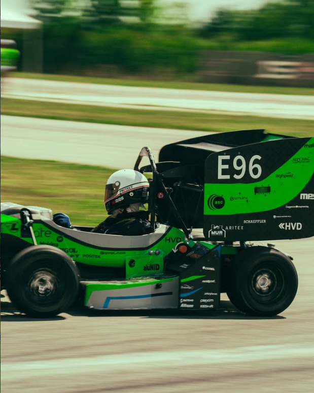
Formula Student Racing Team
 

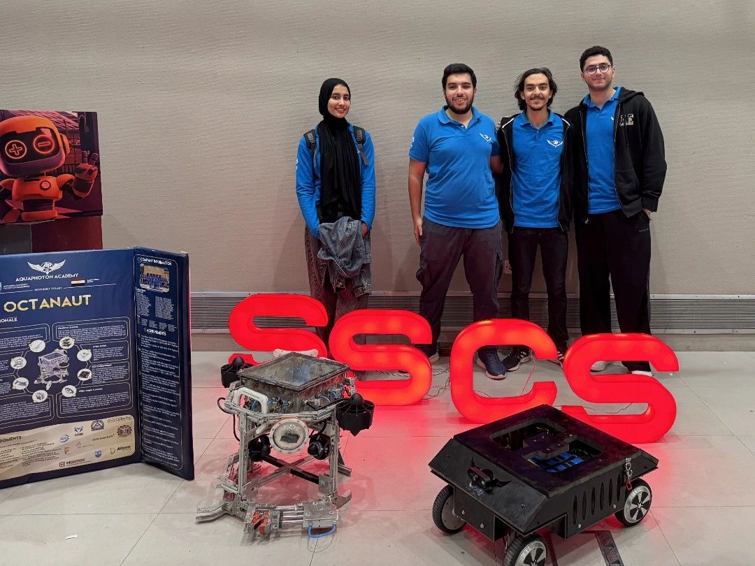
Aquaphoton Academy

READ MORE
Robotics Team Integration
 

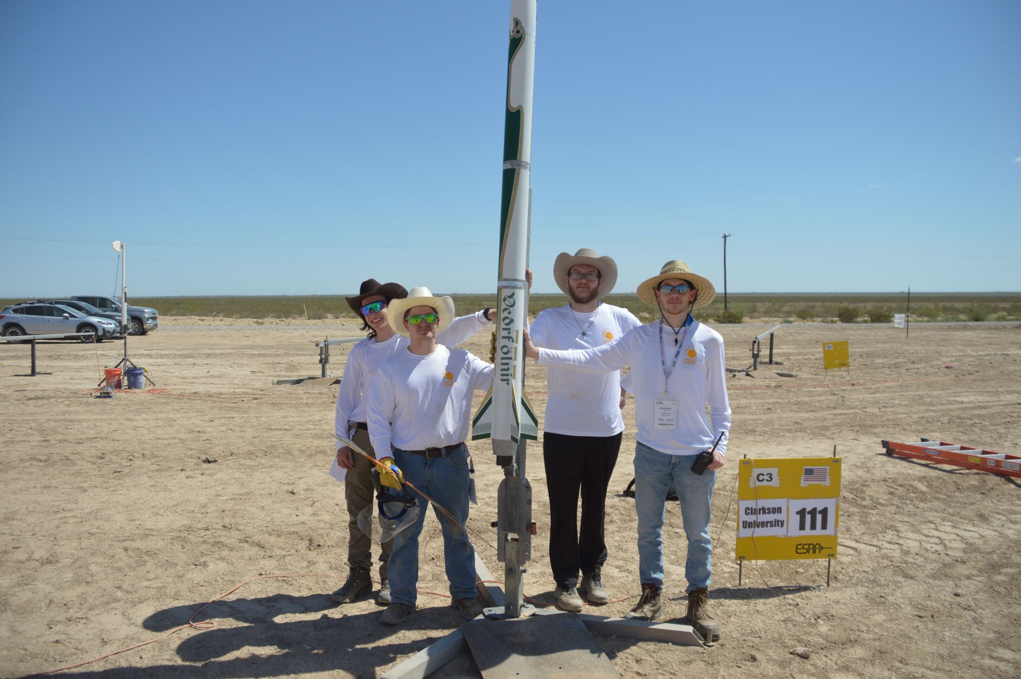
Clarkson University Rocketry

READ MORE
Autonomous Drone Project
 

Etech-racing

READ MORE
Autonomous Drone Project
 

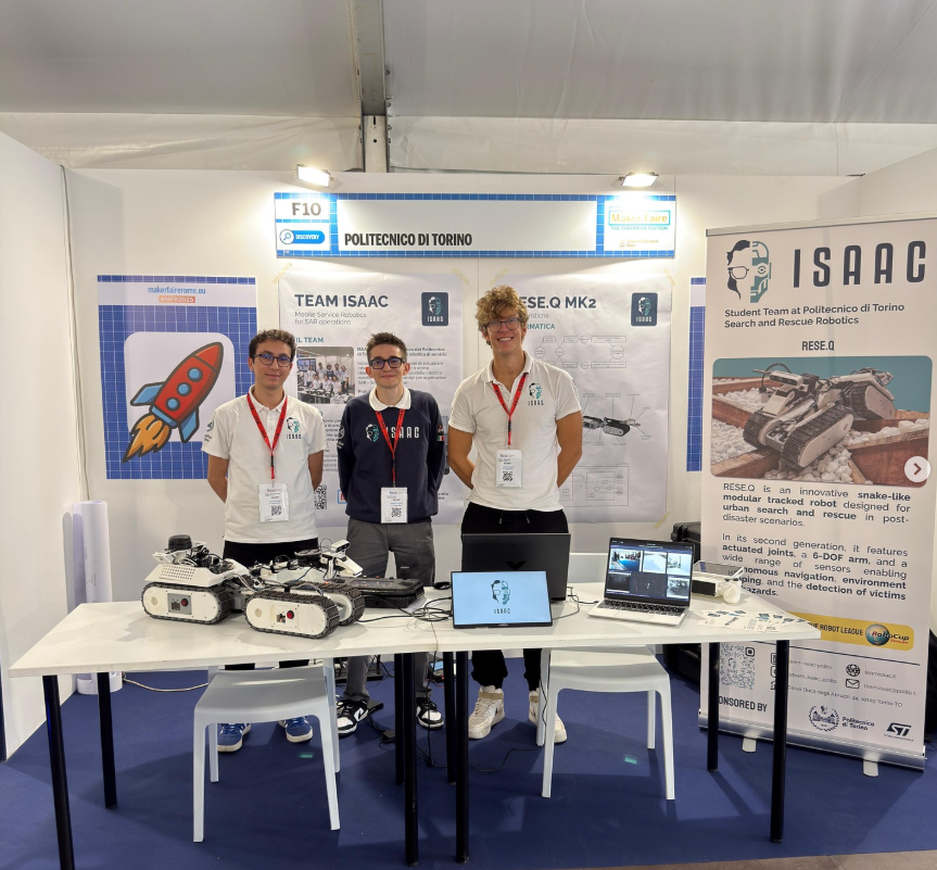
Team ISAAC

READ MORE
Autonomous Drone Project
 

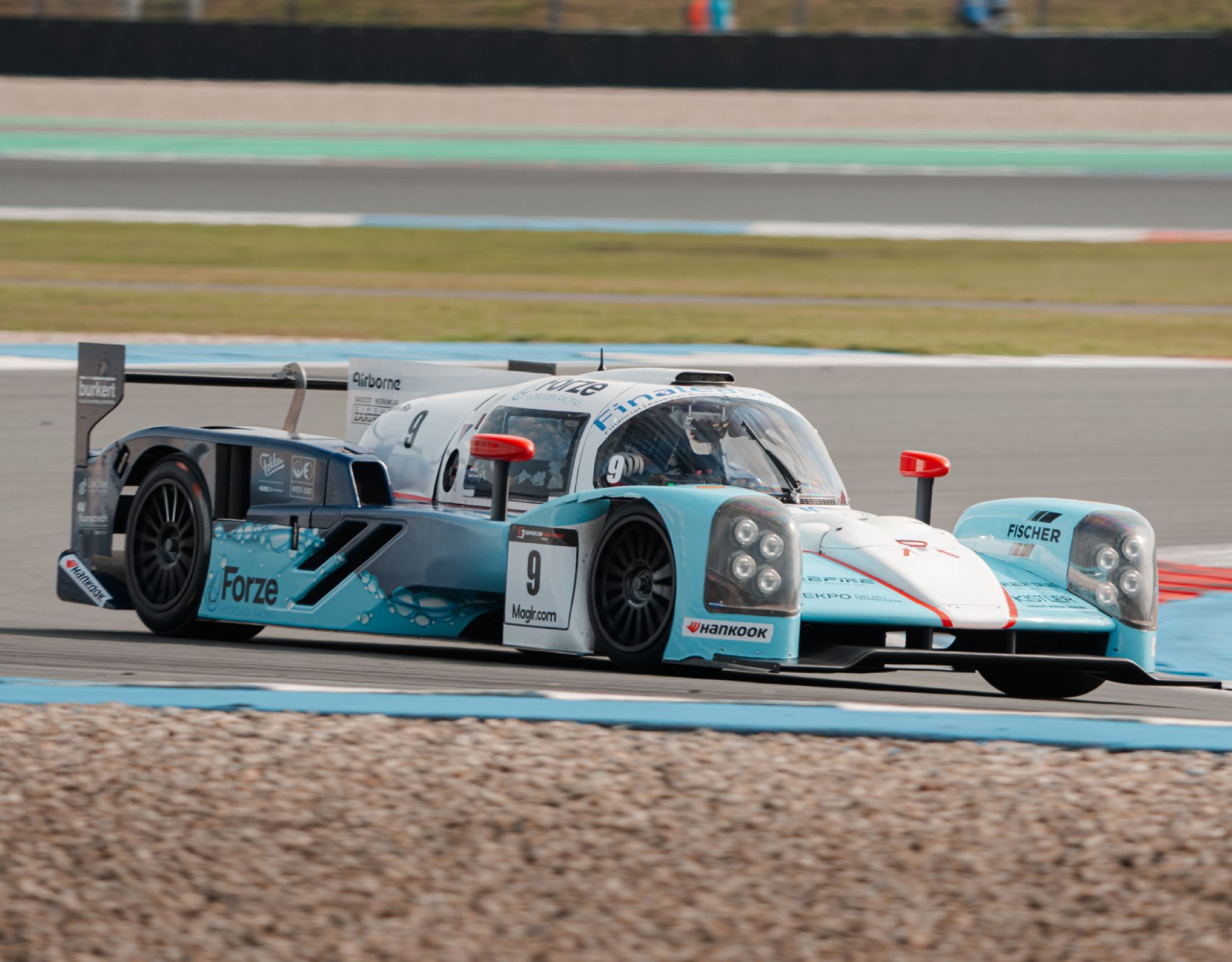
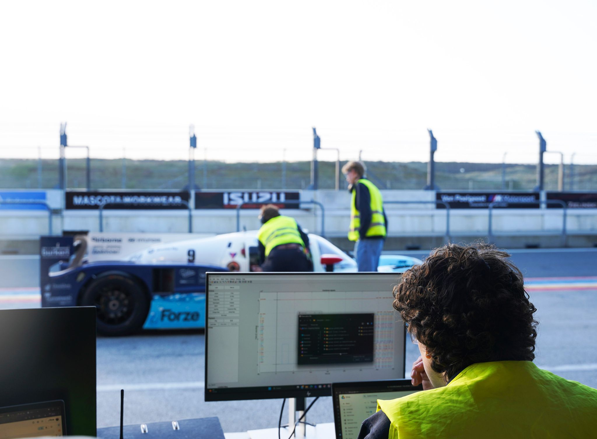
Forze Hydrogen Racing

READ MORE
FAQ
Any currently enrolled students, university research labs, competition teams worldwide and non-profit educational project are also highly welcome.
No, as NextPCB reviews every application case-by-case. We offer a tiered sponsorship model, ranging from substantial discounts to up to 100% full coverage. This sponsorship includs standard PCB prototyping, advanced multilayer fabrication, global component sourcing, and turnkey PCBA assembly.
Yes! For approved high-quality projects, our sponsorship covers shipping costs.
  • Please note: Customs duties, tariffs, and local import taxes are not included in the sponsorship and remain the responsibility of the recipient.
If your project is selected, a member of our team will reach out to you via your academic email within 3–5 business days to discuss the sponsorship quota and next steps.
  • 1. Project Detail & Completeness: A comprehensive project description, including your engineering goals, block diagrams, or preliminary bill of materials (BOM), helps us better understand your technical needs.
  • 2. Project Impact: We highly welcome entries for recognized student competitions, academic research, university lab initiatives, and open-source hardware community projects.
  • 3. NextPCB Brand Exposure: Sharing your journey brings mutual value. We appreciate it when teams can feature the NextPCB logo on the PCB silkscreen, project repositories (e.g., GitHub), or social media updates.
 

Empowering the Next Generation of Hardware Pioneers

Don't let budget constraints hold back your innovation. Submit your project pitch today and let NextPCB do the heavy lifting.

Start Your Application

APPLICATIONS EVALUATED WITHIN 3-5 BUSINESS DAYS

Services
Standard PCB Quote Standard PCB Capabilities Advanced PCB Quote Advanced PCB Capabilities PCB Assembly Quote PCB Assembly Capabilities PCB Stencil Quote
Tools & Resources
HQDFM - DFM Tool Online Gerber Viewer PCB Impedance Calculator PCB Stackups & Impedance KiCad Resource Hub KiCad Download PCB Glossary Blog NextPCB Accelerator Program
About NextPCB
About Us Why Us Payment Methods Shipping Methods Certificate
Distributor
UTSOURCE
Support
Help Center Terms of Service Privacy Policy Return Policy
Payment Methods
Shipping Methods
Certificate
Social Media
NEXTPCB Official youtube NEXTPCB Official Facefook NEXTPCB Official Twitter NEXTPCB Official Instagram NEXTPCB Official Linkedin NEXTPCB Official Tiktok NEXTPCB Official Bksy

©2026 NEXTPCB All Rights Reserved