
 NextPCB Capabilities
Printed Circuit Boards
NextPCB Capabilities
Printed Circuit Boards
 PCB Assembly
 Layer Buildup
 SMD-Stencils
 PCB Design-Aid & Layout
 Mechanics
 Quality
 Drills & Throughplating
 Factory & Certificate
 PCB Assembly Factory Show
Certificate
PCB Assembly Factory Show
Certificate

Support Team
Feedback:
support@nextpcb.com


Stack-up selection on a multilayer board used to be a fairly self-contained engineering call: get the dielectric thickness right, get the impedance math right, done. Whether the material was easy to source rarely entered the conversation. That assumption doesn't hold anymore. CCL and glass fabric prices have been climbing since last year, and board-house lead times have stretched along with them. Pick a PP style that isn't well stocked, and you can turn a routine layout decision into a schedule risk without realizing it until it's too late.
This piece is about one specific call: for standard multilayer designs, defaulting to 7628 as your baseline stack-up removes a meaningful amount of that uncertainty before it ever becomes a problem.
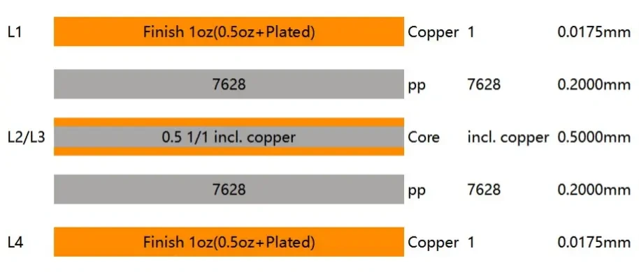
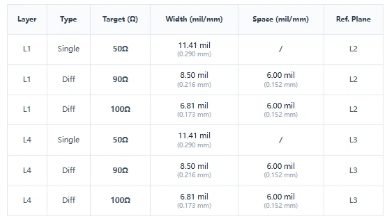
There's a basic rule in engineering: the later a defect surfaces, the more it costs to fix, and the curve isn't linear. Stack-up selection follows the same pattern. Catch a material mismatch at layout, and it's a file revision. Catch it after lamination, and you're looking at a full rework cycle and a production schedule that just fell apart.
So standardizing on a widely available stack-up is really supply chain risk management applied at the earliest possible point — asking "can I actually source this reliably" while you're still drawing the board, not after procurement runs into a wall.
Material usage. A single sheet of 7628 runs about 0.18 mm (7.2 mil). For a typical dielectric thickness target, one sheet of 7628 often does the job that would otherwise take 3–4 sheets of a thinner glass style like 1080. Fewer sheets means lower PP cost on the BOM, plus shorter lay-up time and less risk of resin bleed-out during pressing — a cost that's easy to miss on paper but adds up fast across a production run.
See how 7628 compares against other common PP stack-ups →
Availability. 7628 is the highest-volume glass style in the industry, and it's what most fab houses keep in standing inventory. Thinner or low-loss niche styles — 106 is a good example — tend to be the first thing deprioritized when upstream supply tightens. Sticking with 7628 means your engineering review is far less likely to stall waiting on material, and that matters more right now than it did a year ago.
Mechanical performance. 7628 uses a coarser weave with a higher glass content by weight, which gives it a higher modulus once it's laminated and cured. On larger multilayer boards, that added stiffness helps resist warp and twist during lead-free reflow, which tends to nudge first-pass AOI yield up and cuts down on rework at the SMT stage.
Impedance design margin. A thicker dielectric means you can hit the same target impedance with a wider trace. For 50Ω single-ended, a 7628 stack-up typically lands you at 10–12 mil trace widths, versus 3.5–4.5 mil on a thin-glass build. Narrower traces are more sensitive to copper thickness variation during etch, so the extra width buys real margin against micro-etch opens and shorts.
| Target Impedance | 7628 Stack-Up (∼7.2 mil) | Thin-Glass Stack-Up (∼2.5 mil) |
|---|---|---|
| 50Ω single-ended | 10–12 mil typical | 3.5–4.5 mil typical |
| 90/100Ω differential | 6–8 mil typical | 3.5 mil typical |
Run the numbers for your own design with the PCB Impedance Calculator →
None of the above pays off unless you actually check it before committing to fab.
Impedance back-calculation. Rather than build a sample, measure it, and adjust, run your target impedance against a standard stack-up library up front and settle on trace width and spacing before you start routing.
Panel utilization. 7628 is the base unit most fabs cut their large-format CCL panels against. A poorly planned panel layout that drops utilization below a reasonable threshold — say 75% — is effectively wasted material, and some shops will pass that straight through as a surcharge. Worth catching at design time, not after you've released for production.
DFM/DFA cross-check. A standalone PCB DFM check only covers the bare board. Delivery bottlenecks more often show up where bare-board design meets component footprint and assembly compatibility. Running DFM and DFA checks together at the design stage cuts down a lot of back-and-forth between design and CAM engineering, and surfaces footprint mismatches before they become a line-down problem on the SMT floor.
Upload your Gerbers for a free online check →
Or run a deeper local review with the HQDFM desktop tool →
Nailing the stack-up only solves half the problem — whether the board itself can get built on schedule. The other half is whether the components show up on time. "Board's done, parts aren't" is a familiar situation: the PCB comes off the line and sits waiting on a component that's still in transit.
So schedule management can't stop at stack-up choice. It has to extend one step further — confirming key component inventory against your PCB design parameters before you release to production, locking in what you can lock in early, instead of discovering the gap at the SMT stage.
If you're working against a hard delivery date, it's worth confirming 7628 stock and key component availability directly rather than waiting until you're ready to place the order.
Email: support@nextpcb.com
Phone: +86 755 8364 3663
Business Hours: 7:00 am – 12:00 am (UTC/GMT+8). Outside business hours, we'll do our best to respond within 24 hours.
7628 isn't a breakthrough choice from a technical standpoint — if anything, it's a fairly conservative one. But given where raw material pricing and lead times sit right now, that conservatism is exactly the point: a mature, readily available, high-tolerance stack-up lets you absorb supply chain uncertainty at the design stage, instead of reacting to it during production and delivery.
If this matches what you're seeing on your own projects, here's the fastest way to act on it:
For impedance control needs beyond a standard stack-up, see our PCB Impedance Control Services.
7628 is a woven glass-fabric prepreg (PP) used as the insulating/bonding layer between copper layers in a multilayer PCB. It's one of the most common PP styles in the industry, typically used for standard-thickness dielectric layers in general-purpose multilayer boards, including impedance-controlled designs.
The main difference is glass weave and thickness. 7628 uses a coarser weave and runs about 0.18 mm (7.2 mil) per sheet, while 1080 is a thinner, finer-weave style at roughly 0.06–0.07 mm per sheet. In practice, that means fewer sheets of 7628 are needed to hit a given dielectric thickness, but 1080 (and other thin styles) are sometimes preferred for very thin stack-ups or tight-pitch designs where dielectric thickness has to stay minimal.
It depends on layer count and copper weight, since core and copper thicknesses are also part of the stack, not just the PP. As a general reference, a standard 4-layer 1.6 mm board typically uses 1 sheet of 7628 per PP layer to hit target dielectric thickness. For anything outside a standard 4- or 6-layer build, it's worth running the numbers with a stack-up tool rather than assuming.
Per sheet, price is comparable across common PP styles. The cost advantage comes from sheet count: since one 7628 sheet often replaces 3–4 sheets of a thinner style for the same dielectric thickness, the total PP cost on the BOM tends to come out lower with 7628, along with reduced lay-up labor.
For most standard 50Ω single-ended and 90/100Ω differential targets, yes — 7628 is widely used in impedance-controlled boards. Where it becomes less ideal is when a design needs a very thin dielectric to keep trace width tight for fine-pitch routing, or when a low-loss laminate is required for high-frequency signal integrity. In those cases, a thinner or low-loss PP style is usually the better fit.
Since 2025, CCL and glass fabric pricing has been on an upward trend, and lead times at board houses have stretched. Because 7628 is the highest-volume glass style most fabs keep in standing inventory, designs built around it are less likely to hit sourcing delays compared to designs that rely on thinner or niche PP styles.
Not without a review. Changing dielectric thickness changes the trace width and spacing needed to hit the same target impedance, so any switch to 7628 should go through an impedance recalculation before fabrication — not a straight material swap.
Still, need help? Contact Us: support@nextpcb.com
Need a PCB or PCBA quote? Quote now




