
 Surface


Arya Li, Project Manager at NextPCB.com

 NextPCB Capabilities
Printed Circuit Boards
NextPCB Capabilities
Printed Circuit Boards
 PCB Assembly
 Layer Buildup
 SMD-Stencils
 PCB Design-Aid & Layout
 Mechanics
 Quality
 Drills & Throughplating
 Factory & Certificate
 PCB Assembly Factory Show
Certificate
PCB Assembly Factory Show
Certificate
Support Team
Feedback:
support@nextpcb.com


If you have placed an STM32 microcontroller with an exposed center pad on your PCB and are wondering whether that pad must be connected to ground — the answer is yes, in nearly every practical design. The exposed thermal pad on STM32 QFN and WLCSP packages is electrically connected to the die substrate, which is tied to the internal VSS ground network. Leaving it floating or connecting it to any potential other than ground creates a ground discontinuity that degrades both electrical performance and thermal dissipation simultaneously.
Top view of an STM32 microcontroller on a measurement grid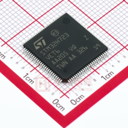
This article explains exactly why the STM32 thermal pad must be grounded, what happens electrically and thermally when it is not, how to implement the via matrix correctly for different package sizes, and what DFM requirements your PCB fabrication partner must meet to ensure a reliable solder joint. For the complete STM32 layout checklist covering impedance routing, PDN architecture, and VIPPO standards across all packages, refer to the STM32 Pinout and Package Guide: High-Speed & HDI Board Layout Best Practices.
The exposed thermal pad (also called the exposed pad, EP, or center pad) is a bare metal area on the underside of QFN, WLCSP, and certain BGA packages. On STM32 devices, this pad is a direct extension of the lead frame that makes physical contact with the silicon die through internal bonding. Its primary engineering functions are:
The thermal pad is present on STM32 packages where the lead frame geometry and die size require direct substrate heat extraction. It is absent on LQFP packages (which use gull-wing leads with no underside contact) and on certain WLCSP variants where VSS redistribution layers serve the equivalent function through dedicated VSS balls.
Yes. STMicroelectronics explicitly specifies in all STM32 package datasheets and application notes that the exposed thermal pad must be soldered to the PCB ground plane. This is not a recommendation — it is an electrical requirement driven by the internal die connection.
The die substrate of every STM32 device is internally bonded to VSS through multiple bond wires connecting the pad to the package ground network. This means:
The ground connection of the thermal pad must be made to the same VSS plane that serves the MCU's VSS signal pins. Connecting the thermal pad ground to a physically separate ground island that is only joined at a remote star point introduces parasitic inductance in the high-frequency ground return path and degrades both SI and EMC performance.
Engineers occasionally ask whether the thermal pad can be left unsoldered during prototyping to simplify hand-assembly. In practice, an unsoldered or floating thermal pad causes a specific and predictable set of failures:
| Failure Mode | Root Cause | Observable Symptom |
|---|---|---|
| ADC noise floor elevated | Substrate floating — VSS reference for analog domain is undefined | ENOB degraded by 2–4 bits; LSB noise visible even with inputs shorted |
| Intermittent resets at high clock speed | Core switching currents have no low-impedance return; VDD/VSS bounce exceeds BOR threshold transiently | System resets at 80 MHz+ but appears stable at 16 MHz internal RC |
| USB enumeration failure | USB_DM/DP common-mode noise increases without solid substrate ground | Device not recognized by host; eye diagram fails compliance test |
| Thermal shutdown in sustained operation | All heat must exit through signal leads; thermal resistance increases 5–10× | Junction temperature exceeds 125°C at moderate load; device enters thermal protection |
| EMC radiated emissions failure | Floating die substrate acts as an antenna for internal switching harmonics | Fail radiated emissions test at clock harmonics (80 MHz, 160 MHz) |
| Package solder joint cracking under thermal cycling | No mechanical anchor from center pad; all stress concentrated on perimeter leads | Signal lead solder joint fracture after 100–200 thermal cycles |
| Package solder joint cracking under thermal cycling | No mechanical anchor from center pad; all stress concentrated on perimeter leads | Signal lead solder joint fracture after 100–200 thermal cycles |
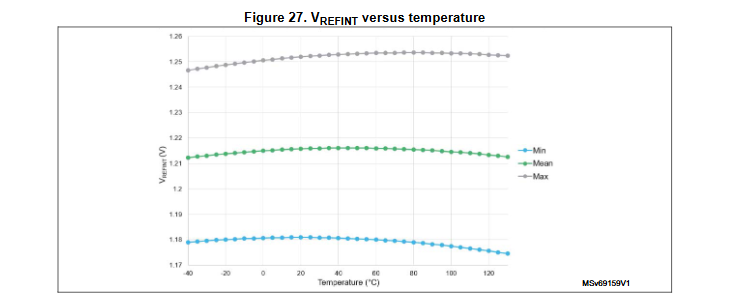
Graph showing V_REFINT versus temperature, illustrating the importance of stable analog references which degrade without proper substrate grounding
 The most commonly encountered failure in prototype bring-up when the thermal pad is unsoldered is the combination of ADC noise and intermittent resets — both of which are difficult to diagnose without knowing the root cause, because they can appear to be firmware or clock configuration issues rather than a PCB assembly defect.
| Package Type | Exposed Thermal Pad | Pad Connection | Example STM32 Devices |
|---|---|---|---|
| QFN (UFQFPN) | Yes — center exposed pad (EP) | Internally tied to VSS; must connect to PCB ground plane | STM32L432 UFQFPN32/48, STM32G0 UFQFPN28/32 |
| WLCSP | Yes — dedicated VSS balls on underside | VSS balls must connect to PCB ground plane through their BGA pads | STM32L476 WLCSP81, STM32U575 WLCSP90 |
| LQFP | No exposed pad | N/A — ground only through VSS signal leads | STM32L476 LQFP64/100/144, STM32U575 LQFP48/64/80/144 |
| UFBGA | No traditional thermal pad — VSS balls distributed across array | VSS balls connect to ground plane through BGA pad footprint | STM32U575 UFBGA132/169 |
| SO8N / SO8 | Some variants have exposed pad on underside | Tied to VSS or VSS2; check per-part datasheet | STM32G0 SO8N (8-pin) |
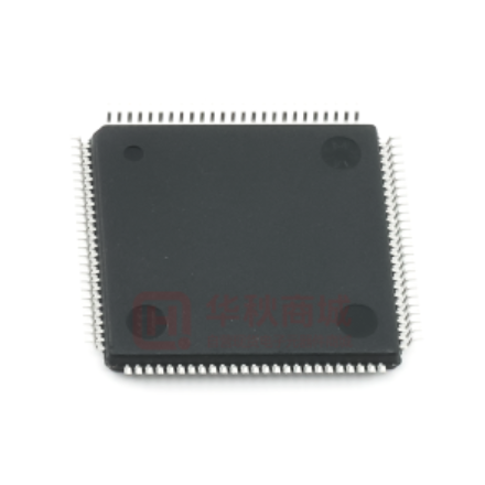
Bottom view of an STM32 LQFP package showing a solid plastic body with no exposed thermal pad
For LQFP packages, there is no exposed thermal pad to connect. The PCB area directly beneath the package body is available for routing low-speed signals or placing decoupling capacitor vias — a useful density advantage on congested boards. However, avoid placing fast-switching signals or SMPS switching nodes in this area, as inductive coupling to the package leads above can occur through the PCB dielectric.
The thermal via matrix is the array of plated through-holes placed within the exposed pad copper area on the PCB. These vias serve two simultaneous functions: they conduct heat from the pad copper down into internal ground planes, and they provide additional current-carrying capacity for the VSS return path. Designing the via matrix correctly requires balancing thermal conductance, solder siphoning risk, and manufacturing capability.
The finished hole diameter of thermal vias must be kept within a specific range to prevent solder paste from flowing down the barrel during reflow — a phenomenon called solder siphoning or wicking.
| Via Finished Hole Diameter | Siphoning Risk | Thermal Conductance | Recommendation |
|---|---|---|---|
| < 0.2 mm | Low | Poor — insufficient copper barrel area | Not recommended; difficult to fabricate reliably |
| 0.2 mm – 0.3 mm | Low to moderate | Good | Preferred range for thermal vias under QFN pads |
| 0.3 mm – 0.5 mm | High | Good to excellent | Acceptable only with VIPPO processing (epoxy fill + copper cap) |
| > 0.5 mm | Very high | Excellent | Not recommended under SMT pads; use only for thermal slugs on non-SMT areas |
Via pitch within the thermal pad should be 0.6 mm to 1.0 mm center-to-center. Tighter spacing risks drill registration errors during fabrication; wider spacing reduces thermal conductance below the target.
The recommended via count depends on the package thermal pad size:
| Package | Thermal Pad Size (approx.) | Recommended Via Array | Via Count |
|---|---|---|---|
| STM32L432 UFQFPN32 | 3.4 × 3.4 mm | 3 × 3 | 9 vias |
| STM32L432 UFQFPN48 | 5.4 × 5.4 mm | 4 × 4 | 16 vias |
| STM32G0 UFQFPN32 | 3.4 × 3.4 mm | 3 × 3 | 9 vias |
| STM32U575 UFQFPN48 | 5.4 × 5.4 mm | 4 × 4 or 5 × 5 | 16–25 vias |
Thermal vias inside the exposed pad must use direct copper connection to the ground plane — never thermal relief spokes. Thermal relief patterns are designed to restrict heat flow during hand soldering to prevent cold joints on signal pads; inside a thermal pad they defeat the entire purpose of the via matrix by dramatically increasing the thermal resistance from pad to plane. Calculate the difference: a solid-fill via connection to a 2 oz copper ground plane achieves θvia of approximately 5–10°C/W per via. A thermal relief connection increases this by 3–5× per via.
The stencil aperture for the exposed thermal pad requires a segmented design — not a single open window matching the full pad area. A solid single-block aperture causes two assembly defects that are difficult to rework after reflow:
| Parameter | Recommended Value | Rationale |
|---|---|---|
| Total solder paste coverage | 50% – 75% of thermal pad area | Sufficient solder volume for electrical and thermal contact; headroom for outgassing |
| Aperture pattern | 3×3 or 4×4 grid of square or rectangular openings | Creates clear outgassing channels between segments during reflow |
| Channel width between segments | 0.2 mm – 0.3 mm | Wide enough for flux vapor escape; narrow enough not to reduce coverage below 50% |
| Individual aperture size | Adjust segment count to achieve 50–75% total coverage with channel widths above | Vary segment count (3×3 vs 4×4) to match pad size rather than changing channel width |
| Aperture alignment to vias | Stencil segments should not directly center over via openings | Prevents solder from flowing directly into via barrels before the pad area wets |
| Stencil thickness | 0.12 mm – 0.15 mm | Consistent with signal pad stencil thickness; avoid local thickness changes for the thermal pad area |
If VIPPO processing is not available from your PCB fabrication partner, via tenting with dry-film solder mask on the top surface of thermal vias is a lower-cost alternative to reduce (but not eliminate) solder siphoning. Tented vias on the top surface block solder from entering the via barrel from above. However, tenting reliability on small via diameters (0.2–0.3 mm) is lower than VIPPO — mask coverage over small holes is inconsistent and can leave partial openings that still allow siphoning. Tenting is acceptable for cost-sensitive applications; VIPPO is required for high-reliability or high-power designs.
VIPPO (Via-In-Pad Plated Over) is a PCB manufacturing process that fills thermal or signal vias with non-conductive epoxy, copper-plates the filled via shut, and then planarizes the surface to create a flat, solderable finish. The result is a via that is mechanically and electrically complete but presents a flat copper surface to the solder paste — identical to a solid pad from the assembly process perspective.
| Scenario | VIPPO Required? | Reason |
|---|---|---|
| Via diameter > 0.3 mm under thermal pad | Yes | High siphoning risk without fill; large open barrel will draw all solder into via |
| High-reliability application (automotive, medical) | Yes | IPC Class 3 assembly standards require void-free solder joints on thermal pads |
| Via diameter 0.2–0.3 mm, standard consumer design | Optional | Siphoning risk is manageable with tenting; VIPPO improves yield but is not mandatory |
| Via diameter 0.2–0.3 mm, high-volume production | Recommended | VIPPO eliminates process variability in stencil printing and reflow; improves yield consistency |
| Signal vias inside BGA or fine-pitch SMT pads | Yes | Any open via under a soldered pad in HDI routing requires VIPPO to prevent solder loss |
| LQFP package (no thermal pad) | Not applicable | No vias under package body required; VIPPO not relevant to pad design |
VIPPO must be explicitly called out in your PCB fabrication notes — it is not a default process and carries an additional cost. When placing an order for PCB assembly that includes QFN components with thermal pads, specify the following in your fabrication drawing notes:
The solder joint under the STM32 thermal pad is invisible to standard optical inspection (AOI) after reflow — the package body covers it entirely. This makes post-assembly verification of the thermal pad joint a specialized process requirement.
2D or 3D X-ray inspection is the standard method for verifying thermal pad solder joint integrity. X-ray penetrates the package body and images the solder distribution under the thermal pad directly. Key parameters to verify:
NextPCB's PCBA service includes X-ray inspection capability for QFN and BGA components, providing void analysis reports that can be reviewed before shipment.
If X-ray inspection is not available, a functional electrical check can detect a floating or poorly soldered thermal pad indirectly:
| Item | Requirement | Verified? |
|---|---|---|
| Thermal pad net assignment | Assigned to VSS (same net as MCU VSS signal pins) | ☐ |
| Ground plane connection | Thermal pad copper poured solid and connected to VSS plane via via matrix — no thermal relief | ☐ |
| Via diameter | 0.2 mm – 0.3 mm finished hole diameter | ☐ |
| Via array pattern | 3×3 minimum (9 vias); 4×4 for pads > 4 mm × 4 mm | ☐ |
| Via pitch | 0.6 mm – 1.0 mm center-to-center | ☐ |
| Stencil aperture | Segmented grid; 50–75% total coverage; channels 0.2–0.3 mm wide | ☐ |
| VIPPO specification | Called out in fab notes if via diameter > 0.3 mm or high-reliability application | ☐ |
| No routing under package | No high-speed or switching signals routed in copper layers directly beneath package body | ☐ |
| Solder mask opening | Solder mask opened over full thermal pad area; no mask over via barrels if tenting is not used | ☐ |
| Post-assembly inspection | X-ray inspection specified for QFN thermal pad void verification; void area target < 25% | ☐ |
| Functional verification | VSS continuity check between thermal pad via and VSS test point; resistance < 1 Ω | ☐ |
NextPCB provides manufacturing support for STM32 QFN designs from prototype to production, including the specialized processes required for thermal pad reliability.
No. The thermal pad is internally bonded to the die VSS substrate. Connecting it to any potential other than VSS (0 V) creates a forward-bias condition on the internal ESD clamping diodes between the substrate and the VDD rail, which can trigger latch-up under transient conditions. It must always be connected to the same VSS net as the MCU's signal ground pins.
Hand-soldering the thermal pad of a QFN package is technically possible but practically unreliable. The pad is inaccessible from the sides of the package and can only be heated indirectly through the PCB from below using a hot-air rework station or reflow oven. Without a controlled solder paste volume from a stencil, the solder joint will be inconsistent. For prototype bring-up, use a stencil and a reflow oven even for single boards — the alternative is undefined behavior from an unsoldered thermal pad that is difficult to diagnose.
The minimum is a 3×3 array (9 vias) for pads up to approximately 4 mm × 4 mm. For larger pads (5 mm × 5 mm and above, as found on UFQFPN48), use a 4×4 array (16 vias). Adding more vias beyond these counts provides diminishing thermal returns while increasing the risk of solder siphoning if via diameters are not tightly controlled. The total thermal resistance improvement from increasing from 9 to 16 vias is typically 15–20% — meaningful but not dramatic compared to the improvement from simply ensuring the pad is soldered at all.
For standard consumer and industrial applications (IPC Class 2), void area below 25% of the total thermal pad area is the commonly accepted limit. For high-reliability applications such as automotive or medical (IPC Class 3), the target is below 10%. STMicroelectronics' own application notes for STM32 QFN packages cite 25% as the threshold above which thermal resistance begins to increase measurably. Voids above 50% will cause perceptible junction temperature elevation under sustained operating load.
Bench testing at room temperature with intermittent operation masks the problems that appear under sustained load or over product lifetime. The failures caused by a floating thermal pad — ADC noise, intermittent resets at high clock speed, EMC emissions — are often load-dependent and temperature-dependent, meaning they appear at full operating conditions or after thermal soak, not during brief bench validation. Mechanical reliability failures from missing the center solder anchor appear after 50–200 thermal cycles, not immediately. The thermal pad must be soldered in all production designs regardless of bench test results.
LQFP packages have no exposed thermal pad, so there is no via matrix or stencil aperture design required. Ground connection is made entirely through the VSS signal leads, which is sufficient for the thermal dissipation of LQFP packages at typical STM32 operating currents. The PCB area beneath the LQFP package body is available for routing, but avoid placing fast-switching signals or power converter switching nodes in copper layers directly beneath the package to prevent inductive coupling to the package leads through the PCB dielectric.

Still, need help? Contact Us: support@nextpcb.com
Need a PCB or PCBA quote? Quote now

