

 NextPCB Capabilities
 PCB Assembly
 Layer Buildup
 SMD-Stencils
 PCB Design-Aid & Layout
 Mechanics
 Surface
 Quality
 Drills & Throughplating
 Factory & Certificate


An undersized trace is one of the few PCB design mistakes you usually can't fix after the boards arrive. It shows up as a warm spot under thermal camera, a voltage drop that throws off a regulator's feedback loop, or in the worst case, a trace that lifts off the laminate under sustained load. All of it traces back to the same root cause: someone guessed at a copper width instead of calculating it.
This guide walks through the IPC-2221 formula that governs trace sizing, shows you how to use NextPCB's free PCB Trace Width Calculator to get an accurate width in seconds, and includes a reference table and worked example so you can sanity-check the numbers by hand. By the end, you'll know exactly how much copper your next power trace needs — and what to do with that number once you have it.
What Is a PCB Trace Width Calculator, and Why It Matters
A PCB trace width calculator is a tool that works backward from your electrical requirements — current, allowable temperature rise, and copper thickness — to tell you the minimum copper width needed to carry that current safely. Instead of eyeballing a trace or copying a width from a previous design, you get a number grounded in the same empirical data that PCB fabricators and design review engineers use.
The stakes are higher than they look on a schematic. Every copper trace has resistance, and every amp of current through that resistance generates heat (P = I2R). If the trace is too narrow for the current it carries, that heat has nowhere to go, and the trace temperature climbs above the rest of the board. On FR-4 laminate, sustained overheating can degrade the solder mask, delaminate the copper, or in extreme cases, open the circuit entirely. A trace that's too wide isn't dangerous, but it wastes board space and can complicate impedance-sensitive routing nearby.
This is exactly the kind of calculation that benefits from a calculator rather than a rule of thumb. "Just make it wider" works until board space runs out; "20 mil per amp" breaks down the moment copper weight or layer location changes. The formula below is what the calculator runs under the hood, so you can see exactly where the numbers come from.
The IPC-2221 Formula Behind the Calculator
IPC-2221 (Generic Standard on Printed Board Design) is the industry-standard reference for PCB trace current-carrying capacity. It replaced the older IPC-D-275 and remains the most widely cited standard for trace width calculations in 2026, even as the more refined IPC-2152 has gained adoption for advanced thermal modeling.
The core formula solves for the cross-sectional area (A) of copper needed for a given current:
A = (I ÷ (k × ΔT0.44))1 ÷ 0.725
Where:
- A is the required cross-sectional area, in square mils
- I is the maximum current the trace must carry, in amps
- ΔT is the allowable temperature rise above ambient, in °C
- k is a constant that depends on whether the trace is on an external or internal layer — 0.048 for external, 0.024 for internal
Once you have the area, converting it to a physical trace width is a simple division by the copper thickness:
W = A ÷ (1.378 × Toz)
Here, W is the trace width in mils, and Toz is the copper weight in ounces per square foot (1 oz copper is 1.378 mils thick). The 0.44 and 0.725 exponents are curve-fitting constants derived from the original IPC-2221 empirical test data — you don't need to memorize them, but they explain why trace width doesn't scale linearly with current. Doubling the current does not simply double the required width; the relationship is closer to a square-root curve, which is exactly why guessing tends to produce traces that are either badly oversized or dangerously narrow.
Internal vs. External Layers: Why Location Changes Everything
Look closely at the k constants above and you'll notice internal layers use exactly half the value of external layers (0.024 vs. 0.048). That's not a rounding coincidence — it reflects a real physical difference in how heat escapes the trace.
External traces, on the top or bottom copper layer, are exposed directly to air. Heat leaves through convection, which is a reasonably efficient process. Internal traces are sandwiched between layers of FR-4 dielectric, which is a poor thermal conductor. The heat generated by an internal trace has to conduct sideways through solid copper and then through the prepreg before it can escape, so the same current raises the internal trace's temperature far more than it would an external one.
The practical result: for identical current and temperature rise targets, an internal trace typically needs roughly twice the width of an external trace on the same board. If your design pushes a meaningful amount of current through an inner layer — a buried power plane split, for instance — it's worth checking both layer options in the calculator rather than assuming the external-layer number will transfer over.
One counterintuitive edge case worth knowing: if your board sits in a sealed, potted, or vacuum enclosure, external traces lose their air-convection advantage entirely. In that situation, use the internal-layer width even for outer-layer traces, since there's no airflow to carry heat away.
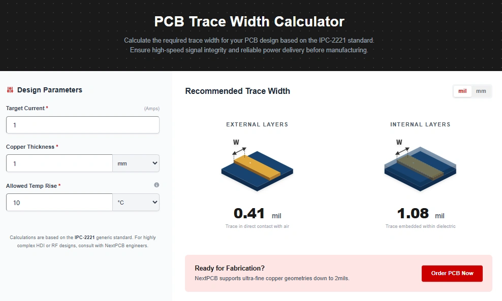
How to Use NextPCB's PCB Trace Width Calculator
Rather than working through the formula by hand every time, you can get an instant result with NextPCB's free PCB Trace Width Calculator. The tool applies the IPC-2221 constants above automatically, so you only need to enter four inputs:
- Maximum current (I) — the highest continuous current the trace will carry, in amps or milliamps
- Copper weight — your board's copper thickness, typically 0.5 oz to 4 oz for standard boards, or higher for heavy-copper designs
- Allowable temperature rise (ΔT) — how many degrees above ambient the trace is permitted to heat up (10°C is the conservative default most engineers start with)
- Layer type — external (outer layer) or internal (inner layer)
The calculator returns the minimum required trace width in both mils and millimeters. If you also enter a trace length, it will chain the result through Ohm's law to give you resistance, voltage drop, and I2R power dissipation for that specific run — useful for checking whether a long power trace will cause a meaningful voltage sag at the load.
One habit worth building early: treat the calculator's output as a floor, not a final answer. IPC-2221 is intentionally conservative and doesn't account for nearby copper pours, ground planes, or components that can help dissipate heat. Most experienced designers add 20–30% margin above the calculated minimum, especially for traces near production tolerance limits or in enclosures with limited airflow.
Worked Example: Sizing a Trace for a 3A Power Rail
To see the formula in action, here's a full walk-through for a common scenario: a 3A power rail on an external layer, 1 oz copper, with a conservative 10°C temperature rise budget, running 60 mm from regulator to load.
Step 1 — Cross-sectional area:
A = (3 ÷ (0.048 × 100.44))1 ÷ 0.725 ≈ 53.8 mils2
Step 2 — Convert to trace width:
W = 53.8 ÷ (1.378 × 1) ≈ 39 mils (about 1.0 mm)
Step 3 — Resistance over the 60 mm run:
Using copper resistivity of 1.7 × 10⁻⁶ Ω·cm and the trace's cross-section, resistance works out to roughly 22 mΩ.
Step 4 — Voltage drop and power loss:
Vdrop = I × R ≈ 3 × 0.022 ≈ 66 mV
Ploss = I2 × R ≈ 9 × 0.022 ≈ 0.2 W
For most 3.3V or 5V rails, a 66 mV drop is negligible. But if this were a 1.0V core supply feeding a sensitive digital load, that same drop would represent nearly 7% of the rail voltage — enough to matter for a tight regulation budget. This is precisely why checking voltage drop alongside trace width, rather than trace width alone, catches problems that a width-only calculation would miss. Running these same four inputs through the calculator above returns the same result in under a second, without the manual unit conversions.
Quick-Reference Table: Trace Width vs. Current
For a fast sanity check during layout, here are IPC-2221 minimum widths for external and internal layers at 1 oz copper and a 10°C temperature rise. These are starting points — always confirm your exact case with the calculator, especially if you're using a non-standard copper weight or temperature budget.
| Current (A) | External Layer Width | Internal Layer Width |
|---|---|---|
| 0.5 A | 4.5 mil (0.11 mm) | 11.8 mil (0.30 mm) |
| 1 A | 11.8 mil (0.30 mm) | 30.8 mil (0.78 mm) |
| 2 A | 30.8 mil (0.78 mm) | 80.0 mil (2.03 mm) |
| 3 A | 53.8 mil (1.37 mm) | 140.0 mil (3.56 mm) |
| 5 A | 108.9 mil (2.77 mm) | 283.2 mil (7.19 mm) |
| 7 A | 173.2 mil (4.40 mm) | 450.5 mil (11.44 mm) |
| 10 A | 283.2 mil (7.19 mm) | 736.8 mil (18.71 mm) |
| 15 A | 495.5 mil (12.59 mm) | 1289.0 mil (32.74 mm) |
| 20 A | 736.8 mil (18.71 mm) | 1916.8 mil (48.69 mm) |
Note the values above 15–20 A: an internal trace at 1 oz copper would need nearly 2 inches of width to carry 20A at a 10°C rise, which is rarely practical. For currents in that range, the usual approach is heavier copper (2 oz or more), a copper pour instead of a discrete trace, or a busbar soldered directly to the board rather than relying on etched copper alone.
Choosing the Right Temperature Rise Budget
The ΔT value you choose has an outsized effect on the result, since it sits inside an exponent in the formula. A few practical guidelines:
- 10°C rise — the conservative default. Appropriate for boards near temperature-sensitive components, military/aerospace designs, or any application where you want generous margin.
- 20°C rise — common for general commercial electronics with adequate enclosure ventilation.
- 30°C+ rise — acceptable for industrial equipment with active cooling or good natural convection, where a warmer trace won't affect nearby parts.
If you're unsure which to use, start at 10°C. It's the safest assumption, and if the resulting trace width doesn't fit your layout, you can revisit the temperature budget deliberately rather than defaulting to a wider trace than necessary out of caution.
IPC-2221 vs. IPC-2152: Which Should You Trust
IPC-2221 remains the most widely referenced standard for trace width calculations, and it's what this calculator — along with most publicly available trace width tools — is built on. But it's worth knowing that a newer standard, IPC-2152, exists and is used for more advanced thermal modeling.
The difference comes down to what each standard accounts for. IPC-2221 treats a trace as if it exists in isolation, with no nearby copper pours, planes, or components affecting heat flow. IPC-2152 factors in board thickness, adjacent copper coverage, and more detailed thermal test data, which typically allows for narrower traces at the same current and temperature rise — often 30–50% narrower in boards with generous copper pours nearby.
In practice: use IPC-2221 as your safety floor during early-stage design, since it's conservative and easy to apply consistently. If board space is tight and a design is otherwise ready, IPC-2152 (or full thermal simulation) can recover some margin — but for the majority of designs, IPC-2221's extra width costs little and buys meaningful reliability headroom. For a deeper dive into IPC-2152 and heavy-copper thermal design specifically, see our related guide on PCB trace width calculation for high-current design and thermal analysis.
From Calculator to Gerber File: Avoiding Fabrication Surprises
A calculated trace width only means something if your fabricator can actually etch it — and reproduce it consistently across the panel. This is the step where a lot of otherwise-correct calculations run into trouble:
- Etching tolerance. Fabrication doesn't reproduce your exact width; there's a manufacturing tolerance, typically around ±10–20% depending on copper weight and trace width. If your calculated minimum is already tight, that tolerance can push a real trace under the safe threshold. This is the core reason to add the 20–30% design margin mentioned earlier, rather than routing to the calculator's bare minimum.
- Heavier copper needs more spacing. As copper weight increases, so does the minimum trace-to-trace spacing the etching process requires for good yield. Moving from 1 oz to 4 oz copper can roughly quadruple the minimum recommended spacing, which affects how densely you can route near a wide power trace.
- Confirm capability before you commit to a width. Every fabricator has minimum and maximum trace width and spacing specifications tied to their process and the copper weight you've selected. Checking these against your calculated width — before finalizing the layout — avoids a DFM rejection or a forced re-route late in the design cycle.
NextPCB's standard process supports copper weights from 0.5 oz up to heavy copper options, with documented minimum trace/spacing capabilities for each. Once you've calculated your trace width here, you can upload your Gerber files directly for an instant PCB fabrication quote and get a fabricator's capability check alongside your pricing — rather than finding out about a spacing conflict after the board is already in production.
One caveat if the trace you're sizing also carries a high-speed signal: current-carrying capacity and characteristic impedance don't always point to the same trace width. A width chosen purely for ampacity can land well outside your target Z0. If that's the case, cross-check the same trace with the PCB Impedance Calculator before finalizing the layout, so you're not solving one constraint at the expense of the other.
Frequently Asked Questions
What happens if I make a trace wider than the calculator's minimum?
Nothing negative from a reliability standpoint — a wider trace simply has more thermal and electrical margin than required. The trade-offs are board space and, in impedance-sensitive designs, a wider trace can shift the characteristic impedance away from your target, so width increases should be deliberate near controlled-impedance nets.
Do I need to widen thermal relief spokes connecting a pad to a ground plane?
Generally no. The IPC-2221 formula is based on long, unsupported traces with no heat-sinking. Thermal relief spokes are short and directly connected to a large copper plane that acts as its own heat sink, so they don't need to match the calculator's output for a comparable trace length.
Is a mil the same as a millimeter?
No — this is a common mix-up. A mil is one-thousandth of an inch (0.0254 mm), not a millimeter. PCB trace widths are conventionally specified in mils in North American design tools and in millimeters in most European and Asian tools, so it's worth double-checking units when comparing a calculator's output to your CAD software's display.
Can this calculator handle currents above 35A?
The original IPC-2221 test data covers up to 35A, 400 mils of trace width, 10–100°C temperature rise, and 0.5–3 oz copper. Outside those ranges, the formula extrapolates rather than relying on tested data, so results above 35A should be treated as a rough estimate. For currents beyond that — common in EV and motor-control applications — heavy copper, copper pours, or soldered busbars are the more reliable design approach, and it's worth validating the design with your fabricator directly.
Why does the calculator give a different answer for the same current at different copper weights?
Copper weight determines trace thickness, and thickness is one of the two dimensions that make up the cross-sectional area the formula solves for. Heavier copper (say, 2 oz instead of 1 oz) means each mil of width carries more cross-sectional area, so the same current can be handled with a narrower trace — roughly half the width when copper weight doubles, all else equal.
Conclusion
Trace width isn't a detail to eyeball and move past — it's one of the few PCB parameters that directly determines whether a board survives its intended current under real operating conditions. The IPC-2221 formula behind this calculator has been the industry reference for exactly that reason: it turns "wide enough" into a specific, defensible number.
Run your current, copper weight, and temperature budget through the PCB Trace Width Calculator before you finalize your layout, add your safety margin, and when your design is ready, bring the same Gerber files straight to NextPCB for an instant fabrication quote — with capability checks built into the process, so the width you calculated is the width you actually get.
If the same trace also carries a high-speed signal, read our companion guide on the PCB Impedance Calculator: Free Tool to Hit Your Target Z0 to check that your current-driven width doesn't push the trace off its target impedance.


