

 NextPCB Capabilities
 PCB Assembly
 Layer Buildup
 SMD-Stencils
 PCB Design-Aid & Layout
 Mechanics
 Surface
 Quality
 Drills & Throughplating
 Factory & Certificate


Above a few hundred megahertz, a PCB trace stops behaving like a simple wire and starts behaving like a transmission line. If its characteristic impedance doesn't match what the driver and receiver expect — usually 50Ω single-ended or 90–100Ω differential — some of the signal reflects back toward the source instead of reaching its destination. The result is ringing, timing jitter, and on high-speed interfaces like PCIe, HDMI, or Ethernet, outright data errors that only show up once the board is populated and running at speed.
Getting impedance right starts well before layout, with the trace geometry itself: width, copper weight, dielectric height, and material dielectric constant all interact to set Z0. This guide explains the formulas behind that relationship, shows you how to use NextPCB's free PCB Impedance Calculator to solve for the right trace width, and walks through two worked examples — one microstrip, one stripline — so you can see exactly how the numbers move.
What Is a PCB Impedance Calculator, and When You Need One
A PCB impedance calculator solves for the characteristic impedance (Z0) of a trace based on its physical geometry — or, run in reverse, solves for the trace width needed to hit a specific target impedance. It takes inputs like trace width, copper thickness, dielectric height, and the substrate's dielectric constant (Dk or εr), and returns the impedance that geometry would produce on a real board.
Not every trace needs this treatment. A slow GPIO signal or a status LED line carries no meaningful risk from impedance mismatch. The traces that do need controlled impedance are the ones carrying high-speed digital or RF/microwave signals: USB, PCIe, HDMI, DDR memory buses, Ethernet, and any RF front-end trace above roughly a few hundred MHz. The general rule of thumb engineers use: if the signal's rise time is fast enough that the trace length becomes a meaningful fraction of the signal's wavelength, it's a transmission line and needs impedance control, not just a wire.
Microstrip vs. Stripline: Two Structures, Two Formulas
PCBs use two dominant transmission line structures, and the calculator handles both — but they don't share a formula, because the electromagnetic environment around the trace is different in each case.
Microstrip traces sit on an outer layer (top or bottom), with a single reference plane below and air above. Because part of the electric field travels through air (εr ≈ 1.0) and part through the dielectric substrate, the effective dielectric constant is lower than the substrate's bulk value, which means faster signal propagation and generally wider traces for a given target impedance. Microstrip is easier to route and simpler to probe, which is why it's the default choice for connector breakout and moderate-speed routing.
Stripline traces are buried between two reference planes on inner layers. The entire electric field stays inside the dielectric, so the effective dielectric constant equals the substrate's full value — this produces better shielding and lower EMI, but also means narrower traces are needed to hit the same target impedance, and propagation is slower (roughly 170–180 ps/inch for stripline vs. 140–150 ps/inch for microstrip on typical FR-4). Stripline needs at least four layers by definition, and etch tolerances on inner layers behave differently than outer-layer etching, which matters when you're trying to hit a tight impedance tolerance.
Most designs end up using both: microstrip for connector breakout and short runs near the board edge, transitioning to stripline for longer high-speed routes that benefit from the extra shielding.
The IPC-2141 Formulas Behind the Calculator
IPC-2141 (Design Guide for High-Speed Controlled Impedance Circuit Boards) provides the closed-form approximations most PCB impedance calculators — including this one — are built on. They're not the last word in precision (more on that below), but they're accurate enough for pre-layout estimates on standard FR-4 designs below about 2 GHz.
Microstrip:
Z0 = (87 ÷ √(εr + 1.41)) × ln(5.98h ÷ (0.8w + t))
Symmetric stripline:
Z0 = (60 ÷ √εr) × ln(4h ÷ (0.67π(0.8w + t)))
Where, in both formulas:
- Z0 is the characteristic impedance, in ohms
- εr is the substrate's dielectric constant (typically 4.2–4.8 for standard FR-4, lower for high-frequency laminates like Rogers materials)
- h is the dielectric height — distance from the signal trace to its reference plane (microstrip), or to the nearer of the two planes (stripline)
- w is the trace width, and t is the copper thickness, both in the same units (mils)
Notice that impedance and trace width move in opposite directions: widening the trace lowers Z0, and narrowing it raises Z0. This is the relationship the calculator solves in reverse — you supply the target impedance and stackup parameters, and it returns the width needed to hit that number, rather than making you iterate by hand.
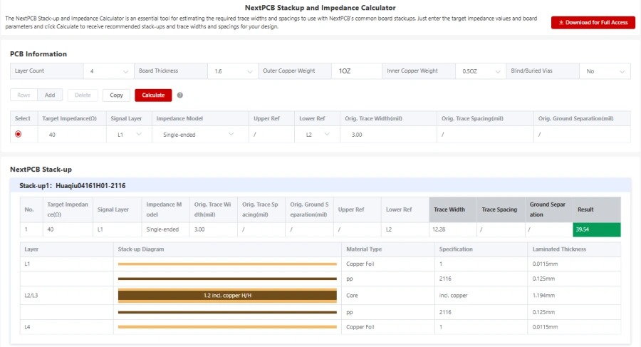
How to Use NextPCB's PCB Impedance Calculator
NextPCB's free PCB Impedance Calculator matches trace width and spacing on your stack to a target impedance, so you can go into layout with dimensions instead of guesses. Typical inputs include:
- Trace type — microstrip or stripline (and, for differential routing, edge-coupled versions of each)
- Dielectric constant (εr) — based on your chosen laminate; standard FR-4 or a high-frequency material like Rogers
- Dielectric height — the distance from trace to reference plane(s) in your stackup
- Copper weight — sets trace thickness, same as in trace width calculations
- Target impedance — the Z0 your interface requires (50Ω single-ended is the most common default; differential interfaces vary by standard)
The calculator returns the trace width that produces your target impedance for the given stackup. If you're still finalizing your layer stackup rather than working with a fixed one, it's worth running a couple of dielectric height options through the calculator before committing — a small stackup adjustment can sometimes get you to a trace width that's easier to route densely, without changing your target impedance at all.
Open the PCB Impedance Calculator
Worked Example: Hitting 50Ω on a Microstrip Trace
Say you're routing a 50Ω single-ended microstrip on standard FR-4 (εr = 4.4), with a 6 mil dielectric height to the first reference plane and 1 oz copper (t ≈ 1.378 mil). Solving the microstrip formula for the width that produces 50Ω:
Z0 = (87 ÷ √(4.4 + 1.41)) × ln(5.98 × 6 ÷ (0.8w + 1.378)) = 50
Solving for w gives a trace width of approximately 9.5 mils. That's a common, easily routable width on a standard 4- or 6-layer stackup, which is part of why 6 mil dielectric height with 1 oz copper is such a widely used starting point for 50Ω microstrip on FR-4 — it lands in a practical width range without requiring an unusual stackup.
If you switch to a thinner dielectric (say, 4 mils instead of 6), the required width for the same 50Ω target drops — the trace has to get narrower to compensate for the closer reference plane. This is exactly the kind of trade-off the calculator is built to resolve quickly, since doing it by hand for every stackup revision gets tedious fast.
Worked Example: Hitting 50Ω on a Stripline Trace
Now the same 50Ω target, but routed as a symmetric stripline — buried between two ground planes with 20 mils total plane-to-plane spacing, same FR-4 and 1 oz copper:
Z0 = (60 ÷ √4.4) × ln(4 × 20 ÷ (0.67π(0.8w + 1.378))) = 50
Solving for w gives approximately 6.5 mils — noticeably narrower than the 9.5 mil microstrip trace needed for the same impedance target. This is the practical consequence of stripline's fully-enclosed dielectric: since the entire field sits inside the substrate rather than partly in air, the trace has to be narrower to reach the same characteristic impedance. It's also why stripline routing tends to be tighter and less forgiving of etch variation — a small width error has a proportionally larger effect on impedance than the same error would on a wider microstrip trace.
Differential Pairs: When Single-Ended Isn't Enough
USB, PCIe, HDMI, and Ethernet don't run single-ended signals at all — they use differential pairs, where two complementary traces (D+ and D−) carry a signal and its inverse, and the receiver looks at the voltage difference between them. This makes the pair far more resistant to common-mode noise, but it introduces a second impedance target: differential impedance (Zdiff), which depends not just on each trace's individual geometry but on how tightly the two traces are coupled to each other.
The relationship is intuitive once you see it: moving the two traces closer together increases electromagnetic coupling between them, which lowers Zdiff; spacing them further apart reduces coupling and raises Zdiff back toward twice the single-ended impedance of an uncoupled trace. Common target values are standardized by interface — 90Ω for USB 2.0/3.0, 100Ω for most PCIe and Ethernet implementations — so the design task becomes finding the width and spacing combination that lands on the interface's specified target, rather than starting from a single-ended number and guessing at a spacing.
Differential pair calculations build on the same microstrip and stripline formulas above, with a coupling correction applied once trace spacing is known. If your board routes any of these interfaces, treat the differential pair geometry as a first-class design input alongside single-ended nets — not something you retrofit onto a layout designed around single-ended assumptions.
Why Calculated Impedance and Manufactured Impedance Don't Always Match
IPC-2141's closed-form formulas are useful, but they're approximations, and it's worth understanding where they lose accuracy so a calculated result doesn't get treated as a guaranteed one:
- They don't model solder mask. A layer of solder mask over a microstrip trace slightly lowers its impedance by increasing the effective dielectric constant around it. Most basic calculators, including simplified IPC-2141 tools, ignore this effect entirely.
- They assume a rectangular trace cross-section. Real etching produces a trapezoidal profile — narrower at the top than the base — and that geometry shift affects impedance slightly, more so at heavier copper weights.
- They use nominal, not measured, material properties. Dielectric constant varies with resin content, frequency, and manufacturing lot, even within the same laminate family.
The practical consequence: expect roughly a 5–10% difference between an analytical calculator's result and what a fabricator's 2D field solver produces for the same stackup. That gap is exactly why controlled-impedance PCB orders go through a fabricator's own stackup verification rather than relying on the calculator's number as a final manufacturing spec — the calculator gets you to a sensible starting geometry, and the fabricator's process confirms (and if needed, fine-tunes) the trace width against their actual laminate and etch data before production.
From Calculator to Controlled-Impedance PCB Order
Once you have a target trace width from the calculator, the next step is making sure your fabricator can actually hold that impedance in production — not just in a spreadsheet. A few things worth confirming before you finalize the layout:
- Impedance tolerance. Standard controlled-impedance manufacturing typically holds ±10% (sometimes ±5–7% for tighter specs); if your interface's timing budget needs tighter control than that, say so on the fabrication order, not after the boards arrive.
- Stackup confirmation. The dielectric height and material you used in the calculator needs to match the actual stackup your fabricator builds — a substitution during production (different prepreg thickness, for instance) shifts impedance even if every other dimension stays the same.
- Note it clearly on your fabrication files. Controlled-impedance nets and their target Z0 should be called out explicitly in your Gerber package or a separate impedance document, not left for the fabricator to infer from trace widths alone.
When your stackup and target impedance are locked in, you can also cross-check trace geometry against current-carrying requirements using the companion PCB Trace Width Calculator — useful when a high-speed trace also needs to carry meaningful current, since the two constraints (impedance and ampacity) don't always agree on an ideal width. Once your design is ready, upload your Gerber files for an instant controlled-impedance PCB quote, with stackup verification built into the fabrication process.
Frequently Asked Questions
What's a typical impedance tolerance I should expect from a fabricator?
Standard controlled-impedance manufacturing commonly holds ±10%. Tighter tolerances, such as ±5–7%, are available for demanding high-speed designs but typically require dedicated stackup verification and may add cost or lead time — confirm this with your fabricator during quoting, not after the design is finalized.
Do I need controlled impedance on every high-speed trace, or just the critical ones?
Just the ones carrying high-speed digital or RF signals where reflections would cause functional problems — clock lines, high-speed serial interfaces, memory buses, and RF front-end traces. Slower control and status signals don't need the same treatment, and treating every net as controlled-impedance adds unnecessary stackup and routing constraints.
Why does my calculated impedance differ from what my fabricator confirms?
Closed-form formulas like IPC-2141 are approximations that don't fully account for solder mask, real etch profile, or exact material properties. A 5–10% gap between a calculator's result and a fabricator's field-solver verification is normal and expected — it's why the fabricator's stackup confirmation, not the calculator alone, is the step that finalizes your production trace width.
Should I use microstrip or stripline for a new high-speed design?
Microstrip is easier to route and route to a connector, and it's the common choice for shorter, moderate-speed nets. Stripline offers better EMI shielding and is generally preferred for longer high-speed routes above roughly 10 Gbps or in EMI-sensitive designs, at the cost of needing inner layers and tighter etch tolerances. Many designs mix both — microstrip for breakout, stripline for the long run.
Conclusion
Impedance mismatches are the kind of problem that's invisible on a schematic and expensive once boards are built and testing at speed — which is exactly why it's worth resolving with a calculator before layout, not after a signal integrity failure in the lab. The IPC-2141 formulas behind this tool give you a reliable starting geometry for microstrip or stripline, and a clear picture of how trace width, dielectric height, and copper weight all trade off against your target Z0.
Run your stackup and target impedance through the PCB Impedance Calculator, cross-check against current requirements with the Trace Width Calculator where needed, and when your design is locked, bring your Gerber files to NextPCB for an instant controlled-impedance quote — with stackup verification built in, so the impedance you calculated is the impedance your board actually delivers.


