
 Surface


Julia Wu - Senior Sales Engineer at NextPCB.com

 NextPCB Capabilities
Printed Circuit Boards
NextPCB Capabilities
Printed Circuit Boards
 PCB Assembly
 Layer Buildup
 SMD-Stencils
 PCB Design-Aid & Layout
 Mechanics
 Quality
 Drills & Throughplating
 Factory & Certificate
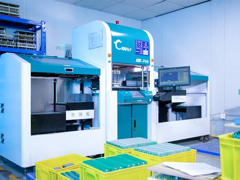
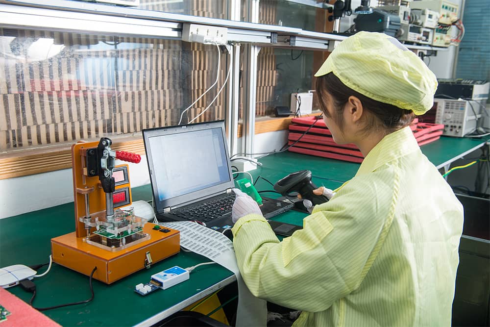
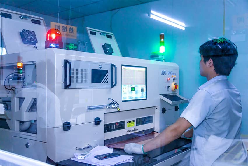
 PCB Assembly Factory Show
Certificate
PCB Assembly Factory Show
Certificate
Support Team
Feedback:
support@nextpcb.com


In hardware design and manufacturing, professional terminology forms the foundation of communication and decision-making. The choice of a "via" type can directly impact BOM costs by 30%, while overlooking the assembly nuances of a "BGA" may lead to catastrophic field failures. To successfully bridge design and volume production, it is essential to thoroughly understand the relationship and technical requirements between a PCB and a PCBA (PCB Assembly). This article not only explains key terms (like SMT, DIP, THT, SMD, BGA, COB, Blind via, Through hole, Buried Via, AOI, X-Ray, ICT, FCT ) but also delves into the core engineering trade-offs that affect product reliability, manufacturability, and total cost.
SMT is central to modern electronics miniaturization. It uses Surface Mount Devices (SMDs), soldering components directly onto PCB pads. This typically saves 60–70% of board space, enables higher-density designs, and suits automated, high-speed production.
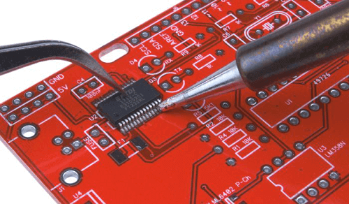
THT requires component leads to be inserted into drilled holes in the PCB and soldered. Although bulkier, it remains indispensable in specific scenarios.
The Engineering Trade-off: Choosing between SMT and THT is fundamentally about balancing space efficiency, production cost, and mechanical/electrical reliability.
SMD Refers to various surface-mount components. Smaller sizes (e.g., 0402, 0201) demand higher placement accuracy and carry increased risk of defects like "tombstoning" during reflow soldering.
BGA packaging is the mainstream choice for high-density integrated circuits. Its solder joints are located beneath the chip, providing hundreds of I/O connections in a very small area.
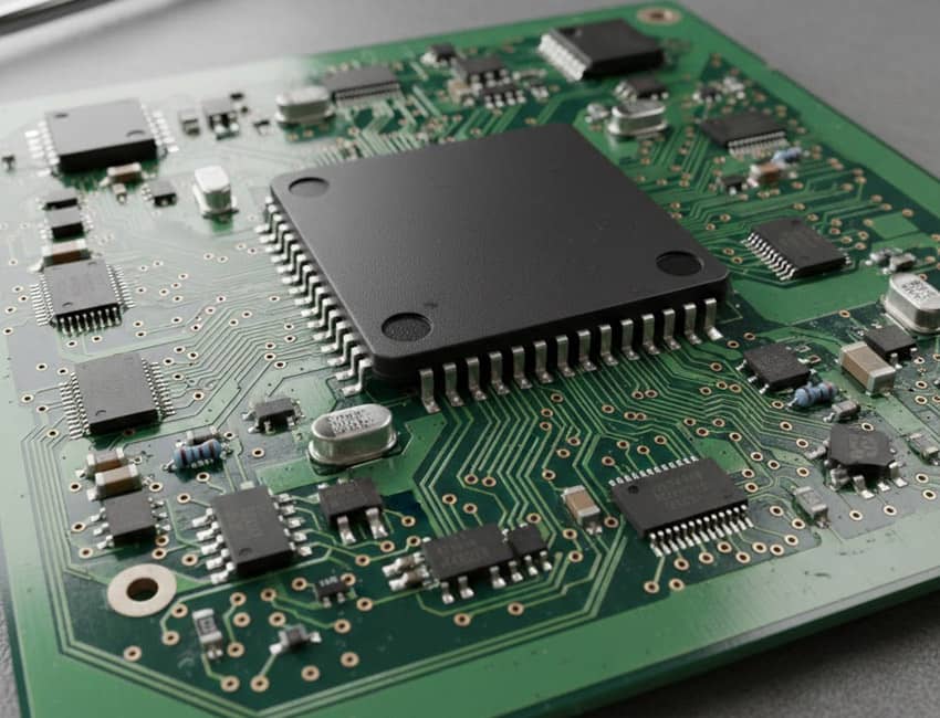
COB packaging bonds bare dies directly to the PCB. It minimizes product profile and cost but results in a non-repairable design, typically used for high-volume, low-cost consumer products.
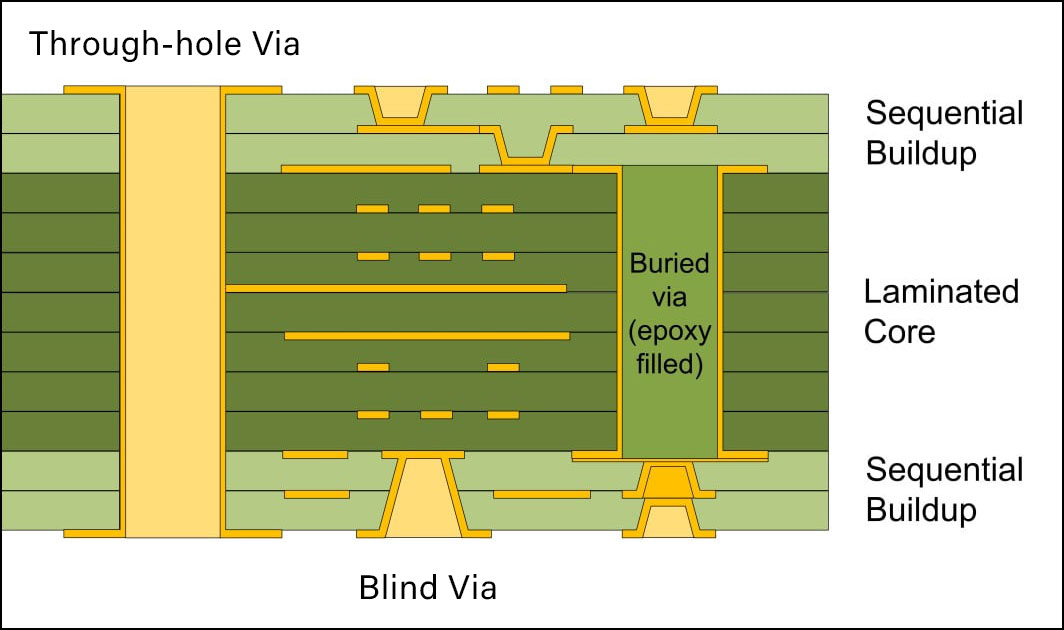
Vias are electrical pathways connecting different layers of a PCB. Their type directly influences stack-up design, routing capability, and manufacturing cost.
| Via Type | Technical Characteristics | Cost Impact | Primary Engineering Purpose |
| Through-Hole Via | Passes through all layers, mechanically drilled | Baseline Cost | General connectivity, good mechanical strength |
| Blind Via | Connects outer layer to inner layers | Increases cost by 1.5–2 times | Essential for HDI designs, frees routing space |
| Buried Via | Connects only between internal layers | Increases cost by 2 times or more | Complex multilayer boards, internal routing density |
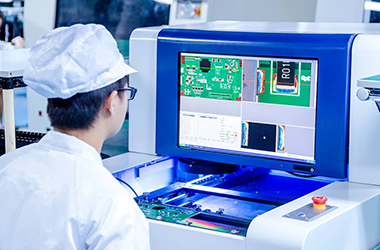
Uses high-definition cameras to quickly detect 2D defects such as placement errors, reversed polarity, and solder bridges. A standard configuration for SMT lines.
Uses a bed-of-nails fixture to verify the electrical performance of on-board components (e.g., resistor values, shorts/opens), ensuring correct soldering and component values.
Simulates the product's real operating environment to verify full board functionality. Serves as the final verification step before product release. Try NextPCB free functional test service.
Primarily used to inspect the solder joint quality of hidden terminations like BGAs and QFNs. An essential method for ensuring the reliability of high-density packages.
Successful PCBA manufacturing is a battle of details. Every decision—from process selection and package awareness to via design and quality inspection—is interconnected, collectively determining the product's performance, reliability, and total cost.
NextPCB specializes in helping engineers transform complex designs into manufacturable, reliable products. Our DFM (Design for Manufacturability) and DFA (Design for Assembly) analysis services identify potential risks before production begins, avoiding costly design iterations.
Get Your Design Right the First Time.

Still, need help? Contact Us: support@nextpcb.com
Need a PCB or PCBA quote? Quote now

