
 Surface


Stacy Lu

 NextPCB Capabilities
Printed Circuit Boards
NextPCB Capabilities
Printed Circuit Boards
 PCB Assembly
 Layer Buildup
 SMD-Stencils
 PCB Design-Aid & Layout
 Mechanics
 Quality
 Drills & Throughplating
 Factory & Certificate
 PCB Assembly Factory Show
Certificate
PCB Assembly Factory Show
Certificate
Support Team
Feedback:
support@nextpcb.com


Every engineer who has moved an ESP32 project from a dev board to a custom PCB has hit the same wall at some point: the code runs, the chip responds, the UART prints cleanly — but Wi-Fi barely reaches two meters, or refuses to connect entirely. The hardware looks right. The software is identical to what worked on the devkit. Yet something is clearly broken.
Nine times out of ten, the problem is the antenna. Not the chip, not the firmware, not the power supply. The antenna — or more precisely, everything around it that should have been left empty.
This guide covers what actually matters when designing ESP32 PCBs for reliable wireless performance: when to use a module versus a bare chip, how to handle the antenna keep-out zone correctly, what the 50 Ω impedance requirement means in practice, how to choose between 2-layer and 4-layer stackups, and the specific layout rules that Espressif publishes but that regularly get missed on first custom designs. At the end, a FAQ section addresses the real questions that come up repeatedly on the Espressif forum and in engineering communities.
Before any layout work begins, the most consequential antenna decision is already in front of you: use a pre-certified ESP32 module, or design around the bare SoC.
The module route — ESP32-WROOM-32E, ESP32-C3-MINI-1, ESP32-S3-WROOM-1, and their equivalents — integrates the antenna, crystal, flash memory, and RF matching network into a shielded unit that has already passed FCC and CE testing. You get a working RF front end without needing RF measurement equipment, simulation software, or a VNA. That is a significant engineering advantage, and it is why modules dominate custom designs at volumes below roughly 10,000 units.
The bare chip route gives you the smallest possible footprint and the lowest per-unit BOM cost at high volume. It also gives you every responsibility: antenna design, impedance matching, crystal selection and load capacitance, PCB stackup specification, and a full RF certification process from scratch. None of these tasks are impossible, but each one is an opportunity for a mistake that kills Wi-Fi performance in ways that are genuinely difficult to debug without a spectrum analyzer or VNA.
| Factor | ESP32 Module | Bare ESP32 Chip |
|---|---|---|
| RF certification | Pre-certified; inherit modular approval | Full certification required (~$5,000–$15,000+) |
| Antenna design | Done; tuned and tested by Espressif | Your responsibility; requires RF expertise |
| Crystal and matching | Included inside the module | External crystal + CLC matching network required |
| PCB footprint | Larger (WROOM-32E: 18 × 25.5 mm) | Smaller (QFN package, 5 × 5 mm or 6 × 6 mm) |
| BOM cost (10K units) | Higher (~$2.00–$3.50 per module) | Lower (~$0.80–$1.50 per chip, plus passives) |
| Debug complexity | Low; RF is handled | High; RF issues are hard to isolate without tools |
| Recommended volume | Prototypes to ~10K units | >10K units where BOM savings justify engineering cost |
For the vast majority of custom ESP32 PCBs — product prototypes, low-to-medium volume IoT devices, one-off tools — modules are the correct answer. The rest of this guide covers both paths, but if you are unsure which route applies to your project, start with a module.
Espressif's module naming encodes the antenna type directly. Understanding this saves time when reading datasheets and evaluating layout options.
| Module | Based On | Antenna Type | Notes |
|---|---|---|---|
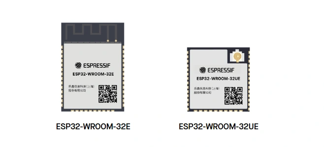
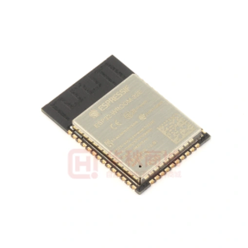
| ESP32-WROOM-32E | ESP32 | PCB trace antenna | Current recommended revision; avoid older -32D |
| ESP32-WROOM-32UE | ESP32 | U.FL connector | "U" suffix always means external antenna connector |
| ESP32-WROVER-E | ESP32 | PCB trace antenna | Adds 8 MB PSRAM; use for camera/display projects |
| ESP32-C3-MINI-1 | ESP32-C3 | PCB trace antenna | Compact 13.2 × 16.6 mm; good for space-constrained designs |
| ESP32-C3-MINI-1U | ESP32-C3 | U.FL connector | For metal enclosures or extended-range deployments |
| ESP32-S3-WROOM-1 | ESP32-S3 | PCB trace antenna | Standard module for S3-based designs |
| ESP32-S3-WROOM-1U | ESP32-S3 | U.FL connector | Use when antenna must be remote from main board |
| ESP32-C6-MINI-1 | ESP32-C6 | PCB trace antenna | Wi-Fi 6 + Zigbee/Thread; newer module family |
The "E" suffix on WROOM modules indicates a revised antenna design with improved RF performance compared to the original revision. Always use "E" variants for new designs. Older modules without the "E" suffix are not recommended for new designs, and some are already reaching end-of-life status in Espressif's product roadmap.
When the product will go into a metal enclosure, near large metallic structures, or needs range beyond what the on-module antenna provides, choose the "U" variant and plan for an external antenna with the appropriate coaxial pigtail and connector. The added BOM cost (connector, cable, antenna) is offset by substantially better RF performance in constrained environments.
This is the section most likely to save you a board respin.
The ESP32 module's PCB trace antenna is a tuned radiating element. Its resonant frequency and radiation pattern depend on the electromagnetic environment immediately around it. Anything conductive within that region — a ground pour, a signal trace, a component, a screw, a battery — changes the effective electrical length of the antenna and detunes it, shifting its resonant frequency away from 2.4 GHz and degrading Wi-Fi and Bluetooth performance.
Espressif's hardware design guidelines specify a mandatory keep-out zone around the antenna. The rules are specific:
The 15 mm requirement is not a conservative guideline you can trim to 12 mm if the layout is tight. At 2.4 GHz, wavelength is 125 mm. Small distances relative to wavelength have significant electrical effects. The keep-out zone is where Espressif's RF engineers have drawn the boundary between acceptable detuning and performance-critical detuning. Violating it is the single most common cause of weak or non-functional Wi-Fi on first custom ESP32 boards, across hundreds of forum posts spanning years of community reports.
In KiCad and Altium, the keep-out region should be defined as a board-level rule area that prohibits copper, components, and vias. This enforcement happens at DRC time, before the board goes to fabrication. In EasyEDA, the equivalent is a no-copper zone on all layers within the region. Whatever the EDA tool, the enforcement needs to be explicit — relying on visual inspection of the layout is not sufficient.
Browse our KiCad Hub — Tutorials, Tools, Downloads, Projects & Resources
The ideal placement puts the ESP32 module at the edge of your PCB with the antenna portion overhanging the board boundary or at minimum flush with the edge. This position gives the antenna an unobstructed view of open space in at least one hemisphere, which is where most of its radiation goes.
When the module must sit toward the center of the board — due to mechanical constraints, connector placement, or enclosure requirements — Espressif's guidelines allow this, but with conditions: the keep-out zone must still be clear on all sides of the antenna, and the base board material must be cut away beneath and beside the antenna to eliminate the dielectric loading effect of the FR4 substrate on the antenna tuning.
| Placement Scenario | Recommendation | RF Impact |
|---|---|---|
| Module at board edge, antenna overhanging | Strongly preferred | Best; antenna sees open space |
| Module at board edge, antenna flush with edge | Acceptable | Good; minor edge effect |
| Module interior, keep-out maintained | Acceptable with board cutout | Moderate; substrate loading reduced by cutout |
| Module interior, no board cutout | Not recommended | Poor; FR4 detunes antenna |
| Module interior, copper beneath antenna | Never | Severe detuning; often total Wi-Fi failure |
| Module in metal enclosure without clearance | Never | Severe signal absorption; metal acts as Faraday cage |
Note that the feed point of the antenna — the point where the antenna connects to the RF circuitry inside the module — determines which end of the module contains the antenna. On WROOM modules, the antenna is on the end opposite the module's pin rows. On MINI modules, the antenna occupies one short edge. Check the mechanical drawing in the datasheet before placing the module, not the photo on the product page.
When the antenna feed point is at the left side of the module, the keep-out region extends left and up. When it is at the right, it extends right and up. Espressif publishes specific keep-out diagrams for both orientations in the hardware design guidelines document for each module family. Use those diagrams directly rather than estimating the keep-out shape from the module photo.
When using a module on a carrier board, you generally do not route an RF trace between the module and an external antenna unless you have chosen the U.FL variant. The RF path is entirely internal to the module. In that case, the antenna-related layout rules are limited to placement and keep-out.
When using the U.FL variant, or when designing a bare-chip board, you must route an RF trace from the chip's LNA_IN pin to the antenna connector or antenna element. This trace must be a controlled-impedance 50 Ω line.
The critical detail here is that the ESP32's RF output is not 50 Ω. The chip presents an impedance of approximately (30+j10) Ω at 2.4 GHz. A 50 Ω antenna connected directly to LNA_IN will see a mismatch that results in VSWR exceeding 3:1, which translates to severe reflection loss and substantially degraded range. The matching network (covered in the next section) handles this impedance transformation, and the 50 Ω feedline connects the matching network output to the antenna.
Espressif's layout guidelines for RF traces are specific and should be followed exactly:
The 50 Ω trace width depends on your PCB stackup. It cannot be specified without knowing the dielectric height, dielectric constant (εr), and copper weight. For a common 2-layer 1.6 mm FR4 board with 1 oz copper and a standard dielectric constant of approximately 4.4, a microstrip RF trace targeting 50 Ω is typically around 3.0–3.2 mm wide. For a 4-layer board where the RF trace is on the top layer with the first ground reference plane at 0.18 mm below, the same target requires a much narrower trace — typically 0.3–0.4 mm depending on the specific stackup.
These numbers vary enough between fabricators and stackup configurations that they should never be taken directly from another project or from a general reference. The correct procedure is to request your PCB fabricator's impedance calculator results for your specific stackup, or to use a tool such as NextPCB's PCB Impedance Calculator with your fabricator's confirmed dielectric parameters.
| Stackup | Layers | Board Thickness | Approx. 50 Ω Trace Width | Notes |
|---|---|---|---|---|
| Standard FR4 2-layer | 2 | 1.6 mm | ~3.0–3.2 mm | Wide trace; needs more board space for RF path |
| Standard FR4 4-layer | 4 | 1.6 mm | ~0.3–0.4 mm | Narrower; easier to route around other components |
| Thin FR4 2-layer | 2 | 0.8 mm | ~1.4–1.6 mm | Used in compact or flexible designs |
Always specify impedance control as a manufacturing requirement when ordering RF boards. NextPCB supports controlled-impedance fabrication and can confirm trace widths for your specific stackup before production. Including this requirement in the fabrication notes eliminates a common source of RF performance variance between prototype iterations. If your design uses BLE alongside Wi-Fi, the same antenna and impedance rules apply; see ESP32 BLE Control in Arduino IDE for a walkthrough of the BLE stack on the same hardware.
The impedance transformation between the ESP32 chip's RF output ((30+j10) Ω) and the 50 Ω antenna feed point is handled by a pi-type CLC network — a shunt capacitor, a series inductor, and a second shunt capacitor placed in sequence between LNA_IN and the antenna.
This network is not optional for bare-chip designs. Connecting the antenna directly to LNA_IN without a matching network produces severe impedance mismatch, high VSWR, and dramatically reduced wireless range. In some cases the radio can still associate with nearby access points at very short range, but throughput and reliability will be poor. At larger distances or with a congested RF environment, the connection may fail entirely.
The component values in the CLC network are not fixed numbers that can be copied from another board and applied directly to yours. They must be determined for your specific PCB, because the effective impedance at the RF pin depends on the trace geometry, board material, stackup, and layout. Espressif provides reference starting values in their hardware design guidelines, but explicitly states that these values must be verified and fine-tuned with RF measurement tools on the actual hardware.
The correct tuning process uses a Vector Network Analyzer (VNA). A NanoVNA, which costs around $50–$100, is sufficient for 2.4 GHz work if handled carefully. The procedure:
For designs using the U.FL antenna connector, the CLC matching network sits between LNA_IN and the U.FL connector. The antenna itself (external) is assumed to be 50 Ω, so only the chip-to-feedline mismatch needs to be corrected. For bare-chip designs with custom PCB antennas, a second matching network may be needed between the feedline and the antenna element, depending on the antenna type.
Component placement for the CLC network is as important as component values. The matching network must be placed as close as possible to the LNA_IN pin, with the shortest practical RF trace between the pin and the first shunt capacitor. Placing the matching network far from the chip effectively extends the unmatched section of the RF path and degrades performance in ways that VNA measurements will not catch unless the probe is at the chip pin itself.
For bare-chip designs, two antenna types are practical for most ESP32 applications: the Inverted-F Antenna (IFA) etched as a PCB trace, and a ceramic chip antenna soldered as a discrete component.
The IFA is Espressif's recommended antenna topology for custom bare-chip designs. It is a tuned trace element that requires no additional components beyond the matching network, costs nothing to add (it is just copper), and provides good radiation efficiency when correctly dimensioned. Its disadvantage is size: an IFA for 2.4 GHz requires approximately 25 × 35 mm of clear PCB area, and this must be free of copper on all layers, not just the top layer.
The MIFA (Meandered IFA) is a space-saving variant that reduces the antenna footprint by folding the antenna trace back on itself. It can fit in approximately 20 × 30 mm, but performance degrades somewhat with reduced ground plane size, and mutual coupling between the meandered sections is harder to control.
Chip antennas (ceramic patch or multilayer antennas in 0402 or 0603 packages) are useful when board dimensions do not allow the minimum IFA footprint. They are matched to a defined impedance (usually 50 Ω) and include the antenna element in a compact component. The trade-off is that chip antennas have lower efficiency than well-designed PCB trace antennas, and they require the same careful RF trace and matching network treatment as any other antenna approach.
| Antenna Type | Min. Board Area | Cost | RF Efficiency | Design Complexity | Best For |
|---|---|---|---|---|---|
| Module PCB antenna | Included in module | Included in module price | High (pre-tuned) | Low (just placement) | Most custom PCBs |
| IFA (bare chip) | ~25 × 35 mm | Free (copper trace) | High (if well designed) | High; needs VNA tuning | High-volume, size-adequate |
| MIFA (bare chip) | ~20 × 30 mm | Free (copper trace) | Medium | High; needs VNA tuning | Space-constrained bare chip |
| Chip antenna | ~10 × 15 mm | $0.20–$1.00 | Medium-low | Medium; matching still needed | Very small boards |
| External antenna (U.FL) | Connector only on PCB | Connector + cable + antenna | High (antenna-dependent) | Low (PCB) / varies (antenna) | Metal enclosures; long range |
A practical note on IFA dimensions: the exact physical length of the antenna trace is determined by the resonant frequency target (2441 MHz center of the 2.4 GHz band), the PCB substrate parameters, and the board thickness. Espressif provides reference dimensions in the hardware design guidelines for their chips, but these must be adjusted if your substrate differs from the reference. Copying dimensions from a development board photo is not reliable — the reference board's substrate parameters may differ from your fabricator's materials in ways that shift the resonant frequency by 50–100 MHz, which meaningfully impacts performance.
Both 2-layer and 4-layer boards can work well for ESP32 designs that use modules. The choice mainly affects RF trace width, routing density, and power integrity — not whether the antenna will work, provided the keep-out zone is respected either way.
For bare-chip designs with custom antennas, 4-layer is preferable for several reasons. The ground reference plane is closer to the RF trace, which means the 50 Ω trace is narrower and easier to route away from other components. The inner planes also provide better power decoupling and EMI shielding for digital signals that could otherwise couple into the RF path.
| Characteristic | 2-Layer | 4-Layer |
|---|---|---|
| Cost | Lower | Higher (~1.5–2× for same board area) |
| 50 Ω trace width | Wide (~3 mm on 1.6 mm FR4) | Narrow (~0.3–0.4 mm) |
| Ground plane quality | Bottom layer; may be interrupted by traces | Dedicated inner ground plane; solid |
| Power integrity | Moderate; requires careful decoupling | Good; inner power plane reduces impedance |
| EMI shielding of digital signals | Limited | Better; inner planes contain fields |
| Routing density | Lower; both layers share signal and ground | Higher; signal layers can be used more freely |
| RF trace routing | Possible, but wide trace limits options | Preferred; narrow trace easier to route |
For module-based designs (the majority of custom ESP32 boards), 2-layer is a perfectly viable choice. Keep the bottom layer as a continuous ground plane with minimal trace routing, place all components on the top layer, use the bottom layer sparingly for signals that cannot be routed on top, and the RF performance of the module will be largely unaffected by the stackup choice.
Antenna problems are the most common cause of ESP32 Wi-Fi failure, but power supply problems are a close second — and they can produce symptoms that look like RF issues: intermittent connections, dropped packets, inability to maintain an association, and in severe cases, the chip resets mid-transmission.
The ESP32's Wi-Fi transmitter draws up to 500 mA in peak bursts during transmission, stepping from microamp-level sleep current to hundreds of milliamps in microseconds. An LDO or power supply that cannot respond quickly enough to this transient allows the rail voltage to dip below the chip's brownout detection threshold (approximately 2.44 V), triggering a reset.
Decoupling capacitor placement is the primary tool for managing this. The rules:
If you observe brownout resets that correlate with Wi-Fi activity, measure the 3.3 V rail with an oscilloscope during a transmission event. Voltage dips exceeding 200–300 mV indicate inadequate decoupling or an LDO that cannot supply sufficient peak current. Adding bulk capacitance or upgrading the LDO current rating typically resolves this.
An ESP32 design that works perfectly on a bench can degrade significantly once enclosed in a product housing. This is not a failure — it is a predictable consequence of putting a dielectric or conductive material near a tuned antenna — but it needs to be accounted for during the design phase rather than discovered during final testing.
Plastic enclosures (ABS, polycarbonate, nylon) shift the antenna's resonant frequency downward, typically by 50–100 MHz at 2.4 GHz. The exact shift depends on the material's dielectric constant, its thickness, and its proximity to the antenna. A common compensation strategy is to design the bare-PCB antenna to resonate slightly high (around 2.50–2.55 GHz) so that it shifts into the correct range once enclosed.
Metal enclosures present a more fundamental problem. Metal reflects and absorbs RF energy. An antenna inside a closed metal enclosure is effectively a Faraday cage that prevents radiation. If a metal housing is required, the U.FL module variant with an external antenna mounted outside or through the housing is the correct approach. A pigtail cable routes from the module's U.FL port to an SMA or RP-SMA bulkhead connector on the enclosure wall, and the external antenna attaches there.
Final product RF testing should always be performed with the PCB inside the actual production enclosure, with all other product components present (battery, connectors, display, etc.). These elements affect the antenna's electromagnetic environment and the resulting range, even when not energized. Projects deployed outdoors — such as a smart irrigation controller inside a weatherproof housing — or installed inside buildings as part of a home automation system both present enclosure conditions that need to be validated before finalising the PCB antenna approach.
Any product with intentional wireless radio emission sold commercially in most markets requires RF certification. For ESP32-based products, the certification approach depends on whether you use a module or the bare chip.
Products using a pre-certified ESP32 module and integrating it per Espressif's hardware design guidelines can often inherit the module's modular approval. This significantly reduces certification cost and time compared to a full radio certification from scratch. However, inheriting modular approval is not automatic: you must follow all of Espressif's integration requirements (keep-out zones, placement rules, labelling), and the extent to which you can claim the module's certification depends on the regulatory body and the specific certification obtained.
| Certification | Region | Module Route | Bare Chip Route |
|---|---|---|---|
| FCC (Part 15) | USA | Modular approval; follow integration rules | Full certification required; ~$5,000–$15,000 |
| CE (RED Directive) | Europe | Module DoC; TCF documentation | Full notified body testing required |
| TELEC (MIC) | Japan | Module certification inherited with conditions | Full certification required |
| SRRC | China | Module pre-approved by some vendors | Full certification required |
Even with a pre-certified module, most certification bodies require that the integration does not alter the RF characteristics of the module. Violating the keep-out zone, placing the module inside a metal enclosure without proper antenna routing, or adding an external amplifier invalidates modular approval and requires a full re-certification. This is another reason why antenna keep-out compliance is not optional.
Several antenna-related issues that cause RF failures can be caught before the board goes to fabrication if a systematic DFM review is done. These checks take ten to thirty minutes in most EDA tools and can prevent a costly and time-consuming board respin.
The checks most relevant to ESP32 antenna performance:
NextPCB's HQDFM tool can be used to catch antenna keep-out violations and impedance-related issues before submitting a board for fabrication. Running HQDFM on the Gerber files before order placement is particularly useful for catching the automatic copper pour issues that are easy to miss in the EDA tool's own DRC.
The following questions come from threads on the Espressif official forum (esp32.com), electronics engineering communities, and engineering Slack groups. They represent the real friction points that come up repeatedly when designers move from dev board prototypes to custom PCBs.
This is one of the most common presentations of an antenna problem. The RF transceiver and the rest of the chip are separate functional blocks; it is entirely possible for the chip to operate normally in every non-RF function while the Wi-Fi radio is completely non-functional due to an antenna or matching network issue.
The most frequent causes, in rough order of probability:
| Cause | How to Check |
|---|---|
| Copper under antenna keep-out zone | Open PCB layout; verify no copper pours, traces, or vias exist beneath the antenna on any layer |
| Missing or incorrect CLC matching network (bare chip) | Check schematic against Espressif reference design; verify all three components are populated correctly |
| RF trace not at 50 Ω | Calculate trace width for your stackup; remeasure width on Gerber vs. calculated value |
| Crystal frequency error or wrong load capacitance | Replace crystal and load caps with known-good components from a working dev board; if Wi-Fi returns, the original crystal was the problem |
| Open or short circuit in RF trace | Inspect solder joints at LNA_IN pin and matching network components under magnification |
| Power supply unable to sustain Wi-Fi TX current | Measure 3.3 V rail with oscilloscope during Wi-Fi scan; look for voltage dips below 2.5 V |
Yes. The keep-out requirement applies specifically to the antenna portion of the module, not to the entire module footprint. Espressif's guidelines allow routing beneath the module body (the shielded area containing the chip, crystal, and flash), provided those traces stay clear of the antenna region. However, routing under the module shield area is generally not recommended as a first choice; the shielded module sits directly on the board surface, and any trace beneath it that carries noise can couple into the module's ground reference. For critical signal lines, routing around the module is preferable to routing beneath it.
The matching network values that produce the correct impedance transformation on one board are specific to that board's substrate, stackup, trace geometry, and component placement. The ESP32 chip's RF output impedance is consistent, but everything between the chip pin and the antenna varies with the physical PCB. A matching network tuned for a 4-layer board with 0.18 mm dielectric height between RF trace and ground will not produce the same result on a 2-layer 1.6 mm FR4 board. The values must be verified and adjusted with a VNA on your actual hardware. This is explicitly stated in Espressif's hardware design guidelines and is a very common source of confusion on the forum.
Not exactly. The module itself is pre-certified, and integrating it per Espressif's guidelines often allows the end product to inherit that modular approval without a full re-certification. But this inheritance is conditional: the keep-out zone must be maintained, the module must be integrated per the guidelines, and the labelling requirements must be followed. If the integration violates any of these conditions — even something as seemingly minor as placing a screw or battery near the antenna area — the modular approval may no longer apply. For products sold in markets with specific regulatory requirements (FCC, CE, TELEC), confirm the certification path with a compliance engineer before finalizing the design.
| Possible Cause | Diagnosis | Fix |
|---|---|---|
| Partial keep-out violation | Copper near but not directly under antenna; RSSI below −70 dBm at 2 m | Remove all copper within 15 mm of antenna on all layers |
| Enclosure detuning | Range worse in enclosure than on bare bench | Increase antenna-to-enclosure clearance; consider U.FL + external antenna |
| Matching network drift (component tolerance) | S11 not centered on 2441 MHz; measure with NanoVNA | Retune matching values; use tighter-tolerance RF components |
| Power supply voltage sag during TX | Dropouts correlate with high-throughput bursts | Add bulk capacitance; upgrade LDO current rating |
| Nearby metal components (battery, connector, heatsink) | Range worse with battery installed than without | Increase physical separation; reposition antenna or use external |
| PCB antenna resonating at wrong frequency | S11 minimum not at 2441 MHz | Adjust antenna trace length; verify PCB substrate parameters |
Yes, but it comes with trade-offs. The main challenge is that the 50 Ω RF trace on a standard 1.6 mm 2-layer FR4 board is approximately 3 mm wide, which consumes significant board area and makes it harder to route away from other components. The ground plane on the bottom layer may also be less continuous than the dedicated inner plane of a 4-layer board. It is workable, and many production devices use 2-layer bare-chip designs successfully, but it requires more careful layout discipline than the equivalent 4-layer design. If the board size and routing complexity are manageable, 4-layer is the more forgiving choice for RF work.
Espressif recommends at least 15 mm clearance in all directions, including inside the product enclosure. This applies to the PCB antenna keep-out zone around the module, as well as to any metallic structural elements of the housing. If mechanical constraints prevent 15 mm clearance on all sides, switching to the U.FL module variant with an external antenna is the recommended solution. The external antenna can be positioned wherever the enclosure geometry allows adequate clearance, independent of where the main PCB sits.
At 200 units, the module is almost certainly the right choice. The per-unit cost difference between a module and a bare chip plus all required passives, crystal, and external flash is typically $0.50–$1.50 at this volume. On 200 units, that is $100–$300 in BOM savings. Against that, the bare chip route adds RF engineering time, VNA tuning iterations, and a full certification process. Even if you already have the RF expertise in-house, the certification cost alone ($5,000–$15,000 for FCC and CE) exceeds the BOM savings by an order of magnitude. The break-even point where bare chip makes economic sense is generally above 10,000 units, and even then only if certification and engineering costs are amortized across the production run.
You can use the reference values from the hardware design guidelines as starting values and the design may work adequately, particularly if your PCB stackup is close to the reference stackup Espressif used when deriving those values. Many successful bare-chip designs have shipped without formal VNA tuning by using conservative reference values and testing range at varying distances against a known-good module. However, this approach accepts some RF performance penalty. If the product needs to function at the edge of its range specification, or if you are designing for a congested RF environment, the reference values without tuning may not be sufficient. A NanoVNA costs around $50–$100 and pays for itself quickly on any project that involves more than one PCB RF iteration.
Reliable Wi-Fi on a custom ESP32 PCB is not complicated, but it requires attending to a specific set of rules that have no equivalent in purely digital PCB design. The keep-out zone, the 50 Ω feedline, the matching network, and the module placement all need to be correct simultaneously. Any one of them done wrong can produce a board that works in every other respect but fails at the one thing the ESP32 is most commonly chosen for. Following Espressif's hardware design guidelines carefully, running DFM checks before fabrication, and using a module rather than the bare chip until volume justifies otherwise will avoid the most common failure modes and get a reliable product to manufacturing faster.
For PCB fabrication with controlled impedance, proper stackup documentation, and DFM review before production, NextPCB's prototyping service supports the RF-specific requirements that ESP32 antenna designs depend on. Antenna keep-out verification is also available through HQDFM prior to order placement.

Still, need help? Contact Us: support@nextpcb.com
Need a PCB or PCBA quote? Quote now

