CHIP PLACEMENT AND ROUTING RULE
BGA is a commonly used component on PCB. Usually, CPU, NORTHBRIDGE, SOUTHBRIDGE, AGP CHIP, CARD BUS CHIP... etc. are mostly packaged in the form of BGA. In short, 80% of high-frequency signals and special signals will be Pull out from this type of package. Therefore, how to handle the routing of the BGA package will have a great impact on important signals.
Small parts usually surrounding the BGA can be divided into several categories according to their importance:
1. bypass.
2. Clock terminal RC circuit.
3. damping (appears in the form of series resistance and row group; for example, memory BUS signal)
4. EMI RC circuit (appears in the form of damping, C, pull height; for example, USB signal).
5. Other special circuits (special circuits added according to different CHIPs; such as the temperature sensing circuit of CPU).
6. Small power circuit group below 40mil (appears in C, L, R, etc.; this kind of circuit often appears near AGP CHIP or CHIP with AGP function, separated by R, L
The same power pack).
7. Pull low R, C.
8. General small circuit group (appears in R, C, Q, U, etc.; no wiring requirements).
9. Pull height R, RP.
The circuits of items 1-6 are usually the focus of placement, and they will be arranged as close as possible to the BGA, which requires special treatment. The seventh item is the second most important circuit, but it will also be ranked closer to the BGA. Items 8 and 9 are general circuits, which are signals that can be connected.
Compared with the priority of the importance of small parts near the BGA, the requirements on ROUTING are as follows:
- a. bypass => When the same side as CHIP, directly connect CHIP pin to bypass and then pull out a bypass to connect to plane; when it is the different side from CHIP, it can share the same via with VCC and GND pin of BGA. The line length should not exceed 100mil.
- b. Clock terminal RC circuit => wire width, wire distance, wire length, or package GND requirements; the wiring should be as short and smooth as possible and try not to cross the VCC separation line.
- c. damping => cable width, line spacing, line length, and packet routing requirements; the routing should be as short as possible, smooth, and one group of groups should not be mixed with other signals.
- d. EMI RC circuit => cable width, line spacing, parallel running line, package GND, and other requirements; completed according to customer requirements.
- e. Other special circuits => cable width, GND package or wiring clearance requirements; completed according to customer requirements.
- f. Small power circuit groups below 40mil => cable width and other requirements; try to complete the surface layer, reserve the inner space for signal lines, and try to avoid the power signal from passing through the layers in the BGA area, causing unnecessary interference.
10. pull low R, C => no special requirements; smooth wiring.
11. General small circuit group => no special requirements; smooth wiring.
12. pull height R, RP => no special requirements; smooth wiring.
In order to more clearly explain the processing of the routing of BGA parts, a series of icons will be described as follows:
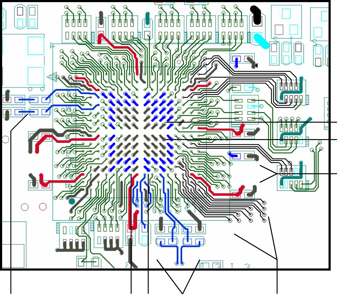
- A. Divide the BGA from the center with a cross, and VIA is hit in the upper left, lower left, upper right, and lower right directions; the cross can be adjusted asymmetrically due to the wiring.
- B. Clock signal cable width and line distance requirements, please try your best when the R and C circuits are on the same side as CHIP
- The above figure is processed.
- C. Please run the USB signal in parallel at the R and C ends.
- D. Bypass Try to connect the CHIP pin to bypass and then enter the plane. Unable to receive bypass.
- Please get off the plane nearby.
- E. For the signal of the BGA component, pull the outer three circles outwards, and keep the original set line width and line spacing; VIA can adjust the wiring sequence in the part entity and 3MM placement forbidden interval, if the wiring has no level requirements, it can be extended Without restriction. Pull the inner circle inward or hit VIA in the middle of PIN and PIN. In addition, the four corners of the BGA should be pulled out by the surface layer as much as possible to reduce the number of VIA in the corners.
- F. The signal of the BGA component should be pulled out as far as possible in a radiation pattern; avoid turning inside.
The BGA routing recommendations made above have the following effects:
- 1. Regular leads are beneficial to the processing of special signals so that all the wiring layers except the surface layer can be completed with the required line width and line spacing.
- 2. The VCC and GND inside the BGA will therefore have better continuity.
- 3. The cross-dividing line in the center of the BGA can be used; when the BGA has more than one internal power supply and it is not easy to cut the VCC layer, it can be processed on the wiring layer (40~80MIL) to the power supply end. Or the CLOCK of the BGA itself, or other signals with larger line width and line spacing, route in the forward direction.
- 4. Good BGA routing and placement can minimize the interference of BGA's own signal.

 NextPCB Capabilities
 PCB Assembly
 Layer Buildup
 SMD-Stencils
 PCB Design-Aid & Layout
 Mechanics
 Quality
 Drills & Throughplating
 Factory & Certificate
 PCB Assembly Factory Show
Certificate
PCB Assembly Factory Show
Certificate


 Surface


lijer
PCB chip placement and wiring issues, first determine the location of the components roughly, ensure that the traces are as short as possible, and then modify according to the specific situation
irhen
Nice page
lisa
This page is professional. It’s likely that edited by an engineer with more than ten years of experience. Thank you for sharing.
shadon
How does a PCB Assembly quote?