NextPCB Capabilities
Printed Circuit Boards
NextPCB Capabilities
Printed Circuit Boards
 PCB Assembly
 Layer Buildup
 SMD-Stencils
 PCB Design-Aid & Layout
 Mechanics
 Quality
 Drills & Throughplating
 Factory & Certificate
 PCB Assembly Factory Show
Certificate
PCB Assembly Factory Show
Certificate
Support Team
Feedback:
support@nextpcb.com


In high-speed multilayer PCB design, traditional double-sided boards often fall short of the stringent requirements for routing signal quality and trace density demanded by modern electronic products. To effectively control impedance, reduce crosstalk, and enhance electromagnetic compatibility (EMC), engineers must rationally plan and configure the PCB stackup structure. Starting from fundamental concepts and integrating common stackup schemes, this article explores how to efficiently implement stackup design in Altium Designer. Additionally, we will address high-frequency design pain points based on actual manufacturing conditions.
When planning internal layers, we first face the choice between "Positive" and "Negative" layers. Understanding the operational mechanisms of both can significantly improve design efficiency and software performance.
Positive Layer: Typically used for signal routing layers. On a positive layer, what you see is what you get—the lines and copper areas you draw represent the actual copper foil that will remain on the final board. Large-area copper pours require the use of Polygon Pour operations.
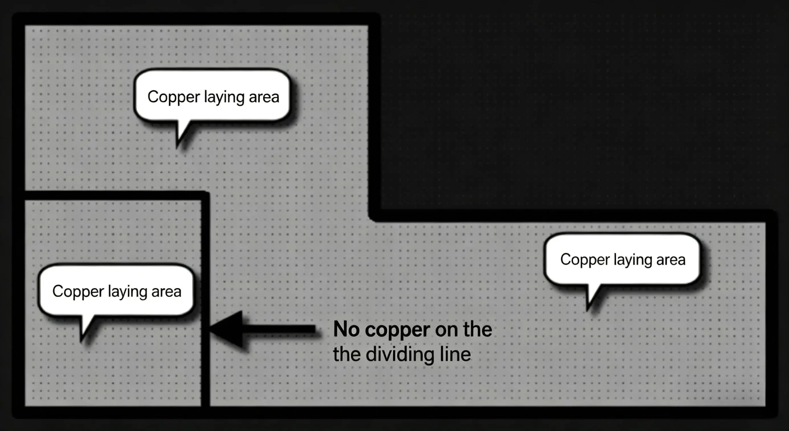
Figure 1: Diagram of a positive layer, where visible elements represent remaining copper foil
Negative Layer: The mechanism is exactly the opposite. Its default state is a layer completely covered with copper foil. The lines we draw on this layer (such as split lines) actually represent copper-free isolation gaps. Designers only need to use lines to divide different regions and assign appropriate nets (such as GND or various power supply voltages) to these specific areas.
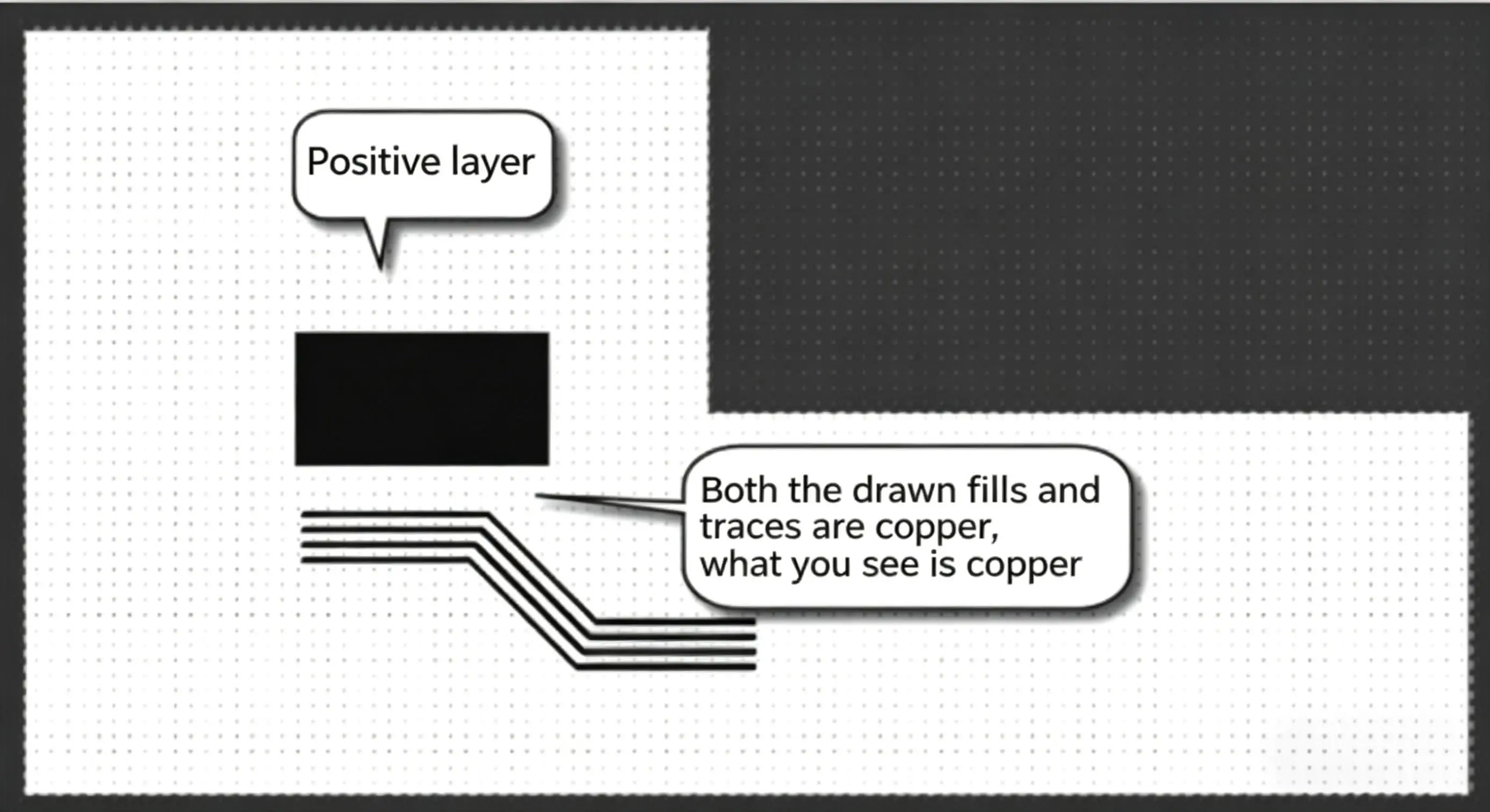
Figure 2: Diagram of a negative layer, where split lines have no copper
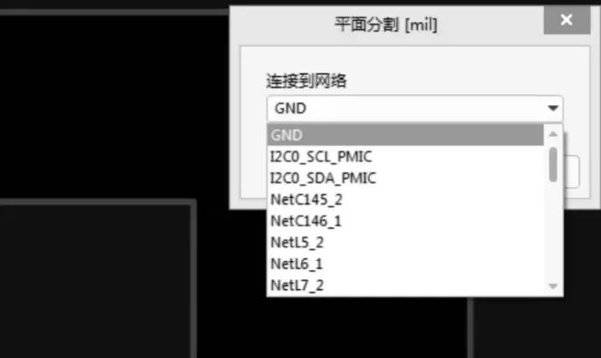
Figure 3: Assigning a specific net (e.g., GND) to a copper pour area after splitting on a negative layer
Engineering Recommendations:
For intermediate Power and Ground (GND) layers, since large areas consist of solid copper planes, it is highly recommended to prioritize negative layers. The greatest advantage is that during subsequent via modifications or split region adjustments, the software does not need to consume massive system resources to recalculate and repour the copper. This significantly optimizes software fluency and reduces file size. Conversely, for signal layers requiring precise routing, you should stick to using positive layers.
With the widespread adoption of high-speed circuits, signal layers and power layers must be properly separated. Deciding whether to use 4 layers, 6 layers, or more is usually based on a comprehensive balance of circuit scale, board outline dimensions, cost budget, and EMC requirements. More layers are not necessarily better; blindly increasing the layer count will exponentially increase manufacturing costs, whereas having too few layers may lead to routing bottlenecks and signal integrity disasters.
When determining the stackup structure, the industry generally adheres to the following fundamental principles:
Based on the above principles, let us analyze the most commonly used 4-layer, 6-layer, and 8-layer board schemes in daily design.
For standard 4-layer boards, the industry typically uses three mainstream stackup schemes:
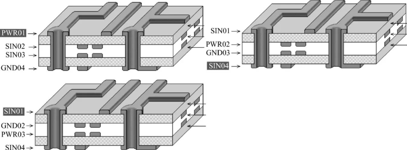
Figure 4: Physical structure diagrams of common 4-layer board stackups
| Option | Layer Diagram | Stack-up | Advantages | Disadvantages |
|---|---|---|---|---|
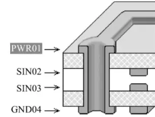
| Option 1 | 1: PWR01 2: SIN02 3: SIN03 4: GND04 |
Mainly designed for shielding by placing Power/GND on top/bottom layers. | (1) Large plane impedance due to distance. (2) Planes are highly incomplete. (3) Poor shielding and discontinuous impedance. |
|
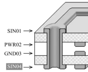
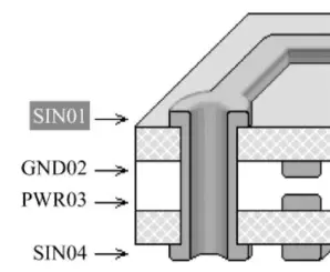
| Option 2 | 1: SIN01 2: GND02 3: PWR03 4: SIN04 |
GND plane under top layer; ideal for critical signals or components on top. | N/A | |
| Option 3 | 1: SIN01 2: PWR02 3: GND03 4: SIN04 |
Similar to Option 2; ideal for critical signals or components on bottom. | N/A |
Conclusion: Through comparison, Scheme 1 has the power and ground planes spaced too far apart, resulting in high plane impedance and making shielding extremely difficult to achieve; therefore, it is rarely used. Usually, we select Scheme 2 or Scheme 3. Please make the correct choice based on the main component placement side and the core stackup principles.
In 6-layer board design, the conflict between routing density and signal isolation becomes more prominent. The following figure illustrates common 6-layer board stackup structures:
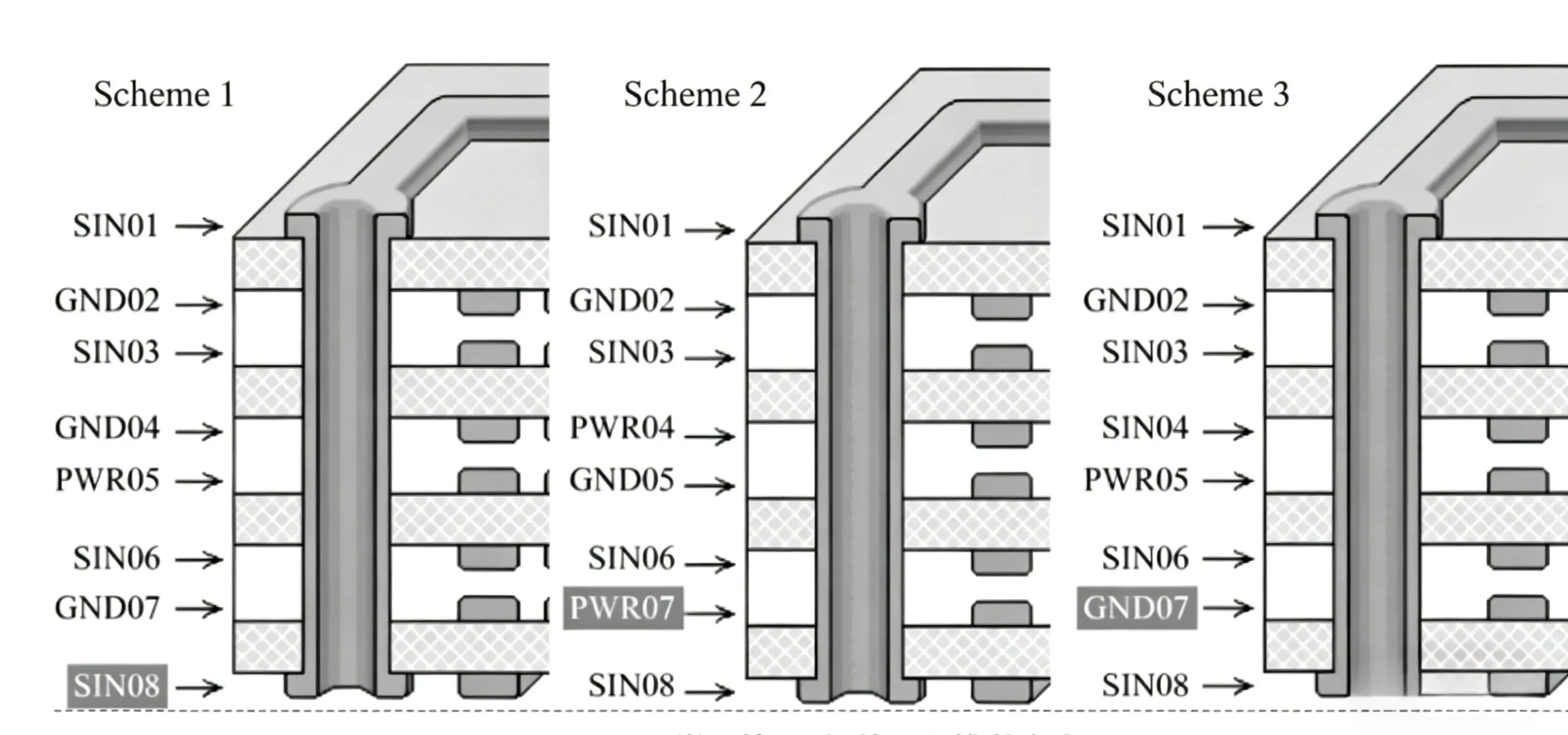
Figure 6: Physical structure diagrams of common 6-layer board stackups
Here is an analysis of the pros and cons for these four 6-layer board schemes:
| Option | Layer Diagram | Stack-up | Advantages | Disadvantages |
|---|---|---|---|---|
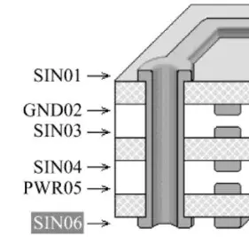
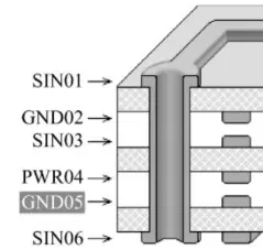
| Option 1 | 1: SIN01 2: GND02 3: SIN03 4: SIN04 5: PWR05 6: SIN06 |
More signal layers; facilitates routing between complex components. | (1) Poor Power/GND coupling. (2) SIN03/04 are adjacent, causing crosstalk; requires staggered routing. |
|
| Option 2 | 1: SIN01 2: SIN02 3: GND03 4: PWR04 5: SIN05 6: SIN06 |
Excellent Power and Ground plane coupling. | Surface signals are adjacent to other signal layers; poor isolation/crosstalk risks. | |
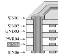
| Option 3 | 1: SIN01 2: GND02 3: SIN03 4: GND04 5: PWR05 6: SIN06 |
(1) Good plane coupling. (2) Each signal layer is adjacent to a plane. (3) SIN03 is shielded by two GND planes for high-speed signals. |
N/A | |
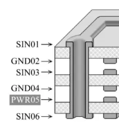
| Option 4 | 1: SIN01 2: GND02 3: SIN03 4: PWR04 5: GND05 6: SIN06 |
(1) Good coupling. (2) All signal layers are adjacent to planes, ensuring isolation. |
N/A |
Conclusion: When prioritizing signal quality, Scheme 3 and Scheme 4 are significantly superior to the first two. However, in actual designs, considering cost and the need for more routing layers, engineers often compromise and choose Scheme 1. If Scheme 1 is selected, special attention must be paid during routing to ensure cross-orthogonal routing between the two adjacent signal layers (SIN03 and SIN04) to minimize crosstalk as much as possible.
For more complex boards, upgrading to an 8-layer board might be necessary. Common 8-layer board stackup recommendation schemes are as follows, where Scheme 1 and Scheme 2 are preferred, and Scheme 3 is acceptable.
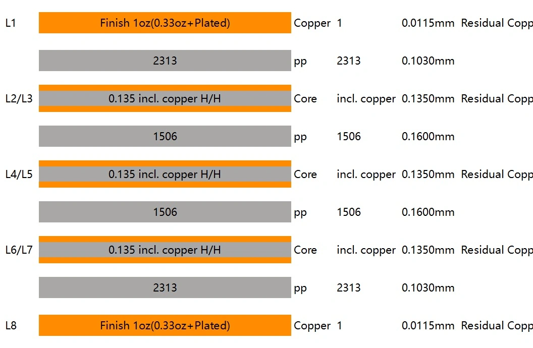
Figure 9: Common 8-layer board stackup recommendation schemes
After establishing the "logical sequence" of the stackup, another crucial factor determining signal quality is the "physical thickness"—namely, the thickness of the dielectric layers (Core and Prepreg, abbreviated as PP). This directly relates to the PCB's impedance control.
In the initial design phase, designers should not simply input arbitrary board thickness data into the software. Instead, they should design based on the actual material library of the PCB manufacturer. Different dielectric constants (Dk), copper thicknesses, and prepreg combinations yield varying impedance results.
Practical Tool Recommendations:
To ensure the design can be successfully manufactured, it is recommended to verify the standard stackup with the board house and calculate the trace widths before setting parameters in Altium Designer:
| Match Your Altium Stackup to NextPCB's Manufacturing Parameters |
After configuring your stackup in Altium, cross-check the dielectric thickness and Er values against NextPCB's available prepreg and core options — so your Altium simulation reflects the actual manufactured board.
Once the physical stackup scheme is confirmed, we can proceed with specific configurations in Altium Designer (AD). Below are the basic operational steps:
Design -> Layer Stack Manager, or directly use the shortcut D + K to access the manager.Properties panel, precisely input the Thickness, material type, and dielectric constant (Dk) according to the stackup data obtained from NextPCB.Pullback distance in the negative layer's properties, for example, setting it to 20mil.To help everyone avoid detours in actual projects, we have compiled a few high-frequency pain-point questions (including advanced topics) that engineers often encounter when planning stackups:
Q1: Can I design an asymmetrical stackup structure to achieve a specific thickness?
A: Strongly discouraged! PCB stackups should strictly maintain central symmetry (including copper thickness, dielectric layer thickness, and copper pour distribution). If the stackup is asymmetrical, the uneven release of internal stress during high-temperature reflow soldering will cause severe board warpage (bow and twist). Mildly, it lowers the yield rate; severely, it leads to pseudo-soldering in high-density components like BGAs.
Q2: The reference ground plane for high-speed differential pairs (like USB 3.0) is split. Does this have an impact?
A: The impact is tremendous. If high-speed signal lines cross a split region in an internal plane (meaning there is no continuous copper plane beneath them), it causes impedance discontinuities and lengthens the signal return path, thereby triggering severe EMI radiation and signal integrity issues. Golden routing rule: Critical signals must never cross splits! If it is absolutely unavoidable, you must place Stitching Capacitors right next to the crossing point to provide a return path.
Q3: Should I place large-area copper pours (ground polygons) in empty areas on signal layers?
A: Copper pouring is generally recommended. Placing ground copper in empty areas (and adding multiple ground vias to connect to internal GND layers) offers three major benefits: First, it balances copper distribution, reducing thermal deformation during reflow soldering; second, it ensures a more uniform chemical reaction during the etching phase, improving trace width precision; third, it provides a certain degree of shielding and heat dissipation.
Q4: When should I upgrade from Through-hole to High-Density Interconnect (HDI) blind/buried via stackups?
A: HDI stackups (such as 1-stage or 2-stage blind/buried vias) cause a steep increase in PCB manufacturing costs and are typically considered only under the following circumstances:
For standard industrial control boards or general-density motherboards, please try to utilize layer counts (e.g., upgrading to 6 or 8 layers) and adopt full through-hole designs to control costs.
Q5: When planning a stackup, what exactly is the difference between Core and Prepreg (PP)? How should they be arranged? (Advanced Topic)
A: The Core is a rigid base material that already has copper foil pressed on both sides; whereas Prepreg (PP) is a gel-like dielectric material that lacks copper foil before lamination. Upon heating, it melts and bonds the adjacent layers.
The standard arrangement rule is: Two adjacent conductive copper layers must be separated by a dielectric (Core or PP). Multilayer boards typically adopt the "foil lamination method" for outer layers. Taking a 4-layer board as an example, the structure usually is: Top Copper Foil + PP + Core (with internal copper on both sides) + PP + Bottom Copper Foil. You cannot stack two Cores directly together without PP, nor can you stack two sheets of PP directly as the primary load-bearing structure.
Q6: How should the inner and outer copper thicknesses be reasonably configured? (Advanced Topic)
A: Unless designing a high-current power board, blindly pursuing thick copper is generally not advised. For standard signal boards, inner layer copper thickness is typically 0.5oz or 1oz. The outer surface copper thickness (base copper) is usually 0.5oz at the factory, and after via plating, the final finished product will reach 1oz or 1.5oz. If the copper is too thick, etching fine-pitch high-speed signal lines easily leads to undercut and out-of-tolerance trace width impedance.
Q7: Why is it always said during stackup that "power planes and ground planes should be as closely adjacent as possible"? (Advanced Topic)
A: Closely adjacent power and ground planes form a natural Inter-plane Capacitance. This capacitance has extremely low Equivalent Series Inductance (ESL) and can provide exceptional decoupling effects for chips at extremely high-frequency bands (hundreds of MHz or even GHz). This significantly lowers the impedance of the Power Distribution Network (PDN), an advantage that cannot be fully replicated no matter how many small SMD capacitors you place in parallel on the board.
Conclusion
PCB stackup design is more than just a few simple settings in EDA software; it is a comprehensive consideration of signal integrity, power integrity, and manufacturing feasibility. In the initial stages of design, combining theoretical principles with the actual process parameters of professional board houses (such as NextPCB) can help engineers avoid many potential hidden dangers, achieving a seamless transition from design to manufacturing.
>>> Recommend reading:
>> Reference: The images in this blog are sourced from the Beihang University (BUAA) Library Catalog System, featuring the entry for "Altium Designer 22 (Chinese Edition): A Practical Guide to Electronic Design" by Zhengyu Zheng et al. (Publishing House of Electronics Industry, 2022, ISBN: 978-7-121-43403-7).
Still, need help? Contact Us: support@nextpcb.com
Need a PCB or PCBA quote? Quote now


 Surface


 .3
.3