
 NextPCB Capabilities
Printed Circuit Boards
NextPCB Capabilities
Printed Circuit Boards
 PCB Assembly
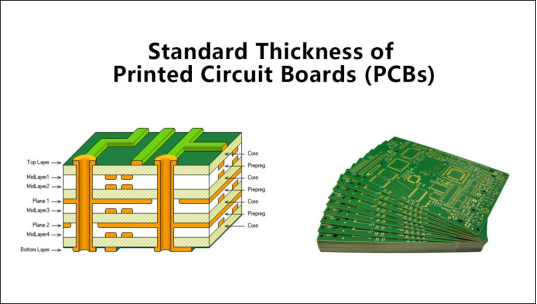
 Layer Buildup
 SMD-Stencils
 PCB Design-Aid & Layout
 Mechanics
 Quality
 Drills & Throughplating
 Factory & Certificate
 PCB Assembly Factory Show
Certificate
PCB Assembly Factory Show
Certificate
Support Team
Feedback:
support@nextpcb.com


PCBs Thickness
PCB thickness refers to the measurement of the board's overall thickness. It is typically specified in millimeters (mm) or sometimes in inches (mil). The thickness of a PCB can vary depending on the specific requirements of the application and the design considerations.
WHAT IS STANDARD PCB THICKNESS?
The standard thickness of a printed circuit board (PCB) can vary depending on the specific application and requirements. However, the most commonly used standard thickness for PCBs is 1.6 millimeters (mm). This thickness is widely accepted and used in various industries, including consumer electronics, telecommunications, automotive, and industrial applications. It provides a good balance between durability, flexibility, and cost-effectiveness. It's worth noting that thinner and thicker PCBs are also available, depending on the specific needs of a project.
1. Standard PCB Copper Thickness
The copper thickness on a PCB is typically measured in ounces (oz) and refers to the weight of copper per square foot. The most common copper thickness is 1oz copper thickness and 2oz copper thickness, and occasionally 0.5 oz (0.7 mils) for low-current applications.
The choice of copper thickness depends on the current carrying capacity required by the circuit. Thicker copper layers can handle higher current levels without excessive heating and voltage drop. For power circuits or circuits with high current requirements, thicker copper layers are generally preferred.
2. Substrate
Substrates and laminates are the foundation or foundation of a PCB. The substrate is a non-conductive dielectric material with a dielectric composite structure. Usually selected according to the dielectric constant.
A common substrate is FR4, which consists of epoxy resin and paper. It is sometimes reinforced with ceramics to increase the dielectric constant. It enables manufacturers to meet performance requirements such as glass transition temperature (the temperature at which heat causes a material to soften and deform). Some standard substrates include FR-1, FR-4 through FR-6, G-10 and G-11, IMS (Insulated Metal Substrate), and more.
3. The Number of PCB Layers
It is very well known and obvious that the layers of PCB affect the thickness. 2-6 layers PCB may have the standard thickness, but eight or more layers of PCB may not fall under the standard thickness of PCB. If a PCB requires more layers, don’t try to use thinner layers to achieve standard PCB thickness because it might become impractical. Allow PCB to be thicker so it can perform its functions.
Sometimes it is not necessary to increase the layers of PCB, so to achieve the required thickness parameters, you can reduce the layers and still manage to achieve the thickness you desire.
4. Signal Type
The type of signal carried on the PCB affects the choice of board material and its thickness. Thicker PCBs with wider copper traces are often required when dealing with high power signals. This is because thicker PCBs can handle higher current levels and provide better heat dissipation.
Thicker PCBs have lower resistance and can handle higher currents without overheating. Wider copper traces also help reduce resistance and prevent overheating. This is important for power-intensive applications that need to carry large amounts of current without damaging the PCB or affecting its performance.
5. Equipment for drilling holes
To be able to make a compact design PCB, the vias route must trace through the board rather than on its surfaces. There are different types of thought holes, through via, micro via, blind via, buried via, and via-in-pad. The density and type of through holes play a major part in determining the thickness of the board.
6. The Operating Environment
The operating environment of PCB thickness refers to the conditions in which the PCB will be used. The thickness of the PCB can affect its performance and reliability in different environments.
The selection of PCB thickness should be based on a thorough evaluation of the specific operating environment, electrical requirements, thermal considerations, and cost constraints of the application.
In conclusion
The choice of PCB thickness depends on several factors. The most commonly used standard copper thickness is 1 oz, which is suitable for most applications. If higher current-carrying capacity is required, you can consider using 2 oz or 3 oz copper layers. Thicker copper layers also provide better heat dissipation. However, thicker copper layers will increase the cost of the PCB. It is important to consider the capabilities and recommendations of the PCB manufacturer when selecting the appropriate copper thickness.
Still, need help? Contact Us: support@nextpcb.com
Need a PCB or PCBA quote? Quote now


 Surface

