
 NextPCB Capabilities
Printed Circuit Boards
NextPCB Capabilities
Printed Circuit Boards
 PCB Assembly
 Layer Buildup
 SMD-Stencils
 PCB Design-Aid & Layout
 Mechanics
 Quality
 Drills & Throughplating
 Factory & Certificate
 PCB Assembly Factory Show
Certificate
PCB Assembly Factory Show
Certificate
Support Team
Feedback:
support@nextpcb.com


Driven by the explosive growth of AI computing, HPC, and high-speed communications, traditional silicon and organic substrates are rapidly approaching their physical and electrical performance bottlenecks. To achieve higher frequencies, lower insertion loss, and higher interconnect densities, the semiconductor industry is shifting from 2D scaling to 3D heterogeneous integration. At the core of this transition is Through Glass Via (TGV) technology. By fabricating vertical conductive vias within a glass substrate, TGV enables high-density electrical connectivity between layers, leveraging the superior electrical and physical properties of glass over traditional materials. TGV has now become a critical enabling technology for next-generation advanced packaging. Global industry leaders including Intel, Samsung, and AMD have already initiated strategic deployments to secure this next-generation manufacturing frontier. This article provides a concise analysis of TGV's core principles, fabrication processes, and its strategic value in the future microelectronics supply chain.
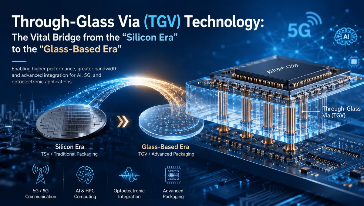
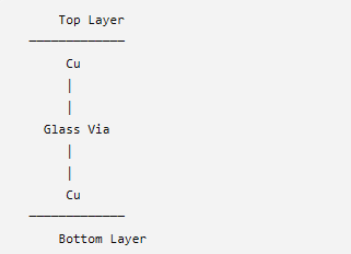
TGV stands for Through Glass Via. It involves forming micro-holes in a glass wafer, glass substrate, or glass interposer, and then filling them with a conductive material (usually copper) to form a vertical interconnect structure. In simple terms, TGV involves "drilling holes" in a glass substrate—not ordinary holes, but precision micro-vias with diameters typically between 10 and 100 micrometers. In advanced packaging applications, tens of thousands or even millions of such vias are often fabricated on each wafer and then metallized to meet the conductivity requirements for high-frequency signal transmission.
Basic structure:
To understand the value of TGV, the best way is to compare it with TSV (silicon through-vias). TSV is the current mainstream vertical interconnect technology and is widely used in advanced packaging solutions such as TSMC's CoWoS and Intel's Foveros. However, TSV has two fundamental problems: high cost and inferior electrical performance. The advantages of TGV over TSV can be clearly shown in the following table:
| Comparison dimension | TGV (through glass via) | TSV (through silicon via) |
|---|---|---|
| Material properties | Insulator | Semiconductor |
| Dielectric constant | About 1/3 of silicon | Reference value |
| Loss factor | 2–3 orders of magnitude lower than silicon | Reference value |
| Insulating layer | No deposition required | Must be deposited |
| Cost | About 1/8 of a silicon-based interposer | Reference value |
| Warpage control | Warpage remains small when thickness is <100 µm | Requires complex process control |
Specifically, TGV's advantages are reflected in the following areas:
Glass is an excellent insulating material, with a dielectric constant of only about one-third of silicon, and a loss factor lower by 2–3 orders of magnitude than silicon. This means that substrate losses and parasitic effects during signal transmission are greatly reduced, effectively ensuring signal integrity. This advantage is especially critical for high-frequency applications such as 5G/6G communications and millimeter-wave radar.
Large-size ultrathin panel glass is easy to source, and TGV does not require depositing an insulating layer on the substrate surface or on the via sidewalls. The fabrication cost of a glass interposer is about one-eighth that of a silicon-based interposer.
TSV technology requires complex oxidation insulating layer deposition, wafer handling of thin wafers, and other steps. TGV does not require these processes, and ultrathin interposers do not need secondary thinning, which greatly simplifies the production process.
Even when the interposer thickness is less than 100 micrometers, the warpage of a TGV substrate remains small, ensuring the stability and reliability of the packaging structure. The coefficient of thermal expansion of glass is closer to that of the wafer, and higher temperature tolerance reduces deformation by 50%.
Glass substrates enable larger packaging sizes than silicon, supporting large-size panel-level production. The spacing between glass vias can be less than 100 micrometers, directly increasing the interconnect density between chips by 10 times.
As stated by Cai Hua, Director of the Key Laboratory of Materials Science for Civil Engineering at the China Academy of Building Materials, “TGV has the potential to replace silicon through-vias in both base material cost and processing cost.”
TGV manufacturing is a precise and complex process, mainly consisting of the following core steps:
Select ultrathin glass with specific composition, thickness, and surface quality. It is typically high-quality borosilicate glass or quartz glass. Glass manufacturers such as Corning, Asahi Glass, and Schott can already mass-produce ultra-large-size panels (larger than 2 m × 2 m) and ultrathin glass (thinner than 50 μm).
This is the most critical step in TGV. Current mainstream via formation methods include sand blasting, photosensitive glass methods, focused discharge methods, plasma etching, laser ablation, electrochemical methods, and laser-induced etching (LIDE).
Among them, laser-induced etching is considered a highly promising technology route. The principle is: using ultrafast pulsed lasers to induce continuous modified regions in glass. The modified glass has a much higher etch rate in acidic or alkaline etchants than the unmodified regions. Based on this selective etching phenomenon, large-scale via structures can be fabricated in glass.
Another technology route is the focused discharge method: place the glass between two electrodes, and by controlling the discharge, locally melt the glass. Using Joule heat, high stress is generated inside the glass, enabling through-hole fabrication in 100–500 μm-thick glass within less than 1 microsecond.
Use wet etching to enlarge the drilled holes, forming TGV trenches, and to repair surface roughness and microcracks caused by laser drilling.
Deposit a metal seed layer on the via walls and inner surfaces, and then use electroplating with metal (mainly copper) to fully fill the through-holes. Void-free copper filling of high-aspect-ratio vias is one of the current core technical bottlenecks.
Remove excess metal through chemical mechanical polishing to make the glass surface flat.
Deposit an insulating layer on the glass surface, form patterns, and electroplate wiring to create the required interconnect circuitry.
Test the completed interconnect wafer, dice it into individual devices for subsequent packaging integration.
As TGV technology has continued to mature, its application scenarios have expanded from laboratory experiments to large-scale industrialization.
| Application Field | Core Value / Technical Advantages | Applications & Quantitative Indicators |
|---|---|---|
| AI Chips & High-Performance Computing (HPC) | Achieves ultra-high bandwidth interconnection between chips; Solves thermal management and signal loss bottlenecks; Features low loss and warpage resistance, solving the deformation and warpage issues of large chips on traditional silicon substrates. | An ideal choice for 3D advanced packaging of AI chips; Improves chip performance by up to 40% while significantly reducing energy consumption. |
| 5G/6G Communications, RF Chips & IoT | Low dielectric loss and high-frequency electrical properties, reducing signal loss; Resistivity reaches 1014 Ω·cm (8 orders of magnitude higher than silicon); RF loss is lower than 0.1 dB/mm @ 60 GHz. | An ideal substrate for RF antennas and millimeter-wave modules (such as RF front-end modules); Applied in 5G millimeter-wave communications and automotive radar (such as 77GHz radar antenna integration); Expected that 50% of new IoT devices will integrate TGV substrates to improve performance and reduce size. |
| Co-Packaged Optics (CPO) & Optical Interconnect | Utilizes the transparent property of glass. | Achieves direct integration of optical modules and computing cores; Used for chip-to-chip optical interconnects and glass-based integrated waveguides. |
| High-End MEMS Sensors | Features good transparency, airtightness, insulation, and corrosion resistance. | Provides highly reliable and miniaturized vacuum packaging solutions for MEMS. |
| Biomedicine & Microfluidics | Glass has good biocompatibility, chemical stability, and optical penetration. | TGV structures can be used for complex microfluidic chips and microfluidic control devices. |
| Other Consumer Electronics & Displays | Based on the wide applicability of TGV technology across multiple fields. | Applied in LED displays, millimeter-wave antennas, and other fields. |
Despite promising prospects, there are still many issues that need to be addressed before TGV can reach large-scale commercial applications.
Glass is a brittle material with low tensile strength. In scenarios with strong temperature variations—such as reflow soldering and thermal shock testing—glass generates significant thermo-mechanical stress. At the same time, the thermal expansion coefficient difference between glass and copper is substantial, which can easily cause delamination or microcracks at the glass–copper interface.
Processes commonly used in TGV manufacturing, such as laser drilling, chemical corrosion, sand blasting, and microfabrication, can easily leave defects in the glass substrate, including microcracks, stress concentration around the via holes, and excessive surface roughness. These processing defects lay hidden risks for later use and may lead to interconnect failure, interface delamination, or cracking of the conductor filling layer.
For vias with diameters ≤ 30 μm and aspect ratios ≥ 10:1, achieving void-free copper filling remains a major technical bottleneck. Electromigration is also one of the main threats to TGV interconnect structures in high current density applications.
Supporting inspection equipment (such as AOI optical inspection for evaluating the uniformity of metal layers on the via sidewalls) has not yet formed industry standards, increasing the complexity of quality control. Challenges in glass core interposer technology mainly focus on three dimensions: TGV reliability, completeness of inspection and evaluation systems, and adhesion of added layers to the surface.
Currently, the leading enterprises in the industry can achieve mass production yields of 95% or higher, but some new entrants are still below 80%. The process complexity and precision requirements mean that scaling up TGV production remains challenging.
TGV technology is not intended to completely replace TSV, but to serve as a complementary approach to solve high-performance interconnect issues in specific scenarios. In the AI era, as computing performance grows dramatically, the "dimension" evolution of packaging technology becomes critical. With its unique balance of electrical, optical, and thermal properties, glass is becoming a core engine driving next-generation semiconductor packaging.
With close collaboration across the upstream and downstream industrial chain—glass manufacturers such as Corning, AGC, and NEG, together with major OSAT/packaging players—TGV is expected to experience explosive growth in the next 3–5 years, as large-size glass panel manufacturing processes mature.
The most core difference lies in the substrate material. TSV (Silicon Through Via) uses silicon as the substrate. Although the process is mature, it has higher losses for high-frequency signals and requires additional insulation layers to prevent short circuits. TGV (Through Glass Via) leverages glass’s strong insulation and low dielectric loss characteristics. It not only reduces signal loss, but also has lower base material cost, making it particularly cost-effective for large-size panel manufacturing.
TGV technology is currently widely used in heterogeneous packaging for high-performance computing (HPC), 5G/6G RF front-end modules, optical-electrical co-packaging (CPO), MEMS sensors, and biological microfluidic chips. Its core advantages are high-speed transmission, optical integration, and high reliability in complex environments.
AI chips have extremely high requirements for bandwidth density and energy efficiency. TGV technology not only enables very high interconnect density, but also achieves shorter routing through a glass substrate. In addition, its excellent heat dissipation performance and lower signal interference help effectively support large-scale Chiplet architectures, significantly improving the performance and energy-efficiency of AI computing systems.
At present, the biggest technical difficulty for TGV lies in the efficiency and quality of micro-hole machining, as well as the consistency of large-scale manufacturing. Although glass has advantages, it is relatively brittle. How to maintain high aspect ratios while ensuring high yields during laser drilling and subsequent metal filling processes is a key focus for global OSAT/packaging manufacturers.
No, TGV technology mainly exists as a complementary solution. In specific scenarios that require extreme high-frequency signal transmission, optical-electrical integration, or thin-and-light, low-cost large-area packaging, glass substrates have advantages that are difficult to replace. Meanwhile, silicon substrates will remain dominant in the short term due to their mature manufacturing ecosystem and compatibility with logic process integration. Both will develop together across different application layers.
Still, need help? Contact Us: support@nextpcb.com
Need a PCB or PCBA quote? Quote now


 Surface

