
 NextPCB Capabilities
Printed Circuit Boards
NextPCB Capabilities
Printed Circuit Boards
 PCB Assembly
 Layer Buildup
 SMD-Stencils
 PCB Design-Aid & Layout
 Mechanics
 Quality
 Drills & Throughplating
 Factory & Certificate
 PCB Assembly Factory Show
Certificate
PCB Assembly Factory Show
Certificate
Support Team
Feedback:
support@nextpcb.com


Table of Contents
For PCB panelization, engineers usually master basic rules, such as panelization with routed gaps (adding horizontal and vertical spacing) and gapless panelization (zero-gap panelization by sharing cutting lines). Connection points typically adopt V-scoring (V-cut) or mouse bites (stamp holes) based on outline routing requirements, supplemented by breakaway tabs (process edges), positioning holes, and Mark points. However, in actual manufacturing scenarios, PCBs come in various shapes, and simply applying standard rules often leads to Design for Manufacturability (DFM) defects. An in-depth understanding of production processes—especially CNC milling (routing), outline routing restrictions, and mass production stability—is key to handling complex irregular board panelization. Reasonable panelization design can effectively avoid risks such as processing burrs, board breakage, and formability failure.
Overview: Successful PCB panelization goes beyond simply fitting shapes together based on basic outline rules. A robust panelization strategy must comprehensively evaluate CNC tool paths, connection methods, board-edge components, castellated holes, and potential assembly interference. Different board shapes dictate completely differently tailored panelization strategies. Below are panelization optimization cases for different PCB shapes, deeply analyzing the panelization logic from an engineering perspective.
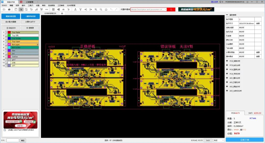
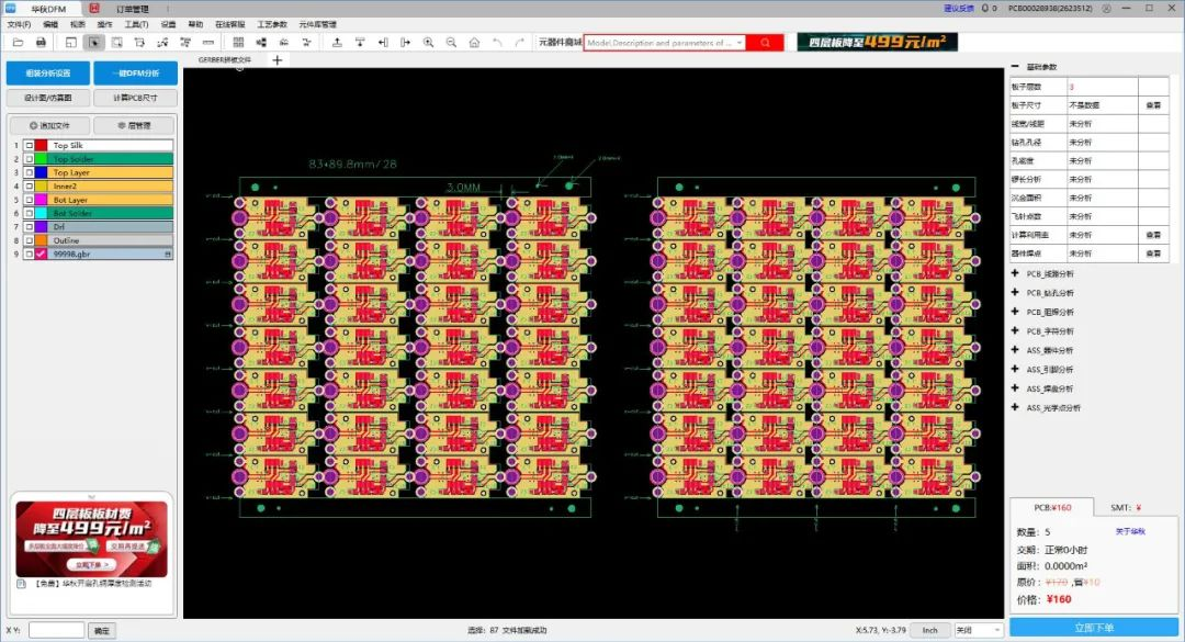
1) When adopting the CNC milling (routing) + V-scoring combination panelization method, attention must be paid to the flatness of the outer contour. As shown in the panelization below, if gapless panelization is adopted on all sides (top, bottom, left, and right), but the top and bottom outline positions of the single PCB have grooves or non-linear structures, this zero-gap design is unreasonable. The processing risk lies in: V-scoring tools cannot handle non-linear paths, and if the groove is smaller than the milling cutter diameter (usually 0.8mm-2.4mm), it cannot be milled. Forced processing will result in obvious burr residues (see left image). Therefore, for this type of outline, a 2mm routed gap should be reserved in the top and bottom directions. Abandon V-scoring and adopt routed gaps instead, utilizing the 2mm spacing to reserve tool path space for the milling cutter, thereby ensuring the finished edges are flat and burr-free (see right image).
2) For irregular PCBs such as L-shapes, to improve board material utilization and reduce costs, engineers often adopt "inverted panelization" (rotated panelization). However, in L-shaped inverted gapless panelization, the left and right V-scoring lines cannot connect on the same horizontal line, causing the V-scoring tool to be unable to pass through. If "jump V-scoring" technology is forcibly used, it will not only significantly increase processing costs but also easily cause tool joint defects (see right image). The optimized solution is to reserve a 2mm routed gap in the left and right directions, replacing V-scoring with CNC milling, which resolves the non-formability issue and ensures outline dimensional accuracy (see left image). Common Mistake: Focusing strictly on maximizing material utilization rate without evaluating the routing and forming risks often leads to unmanufacturable panels.
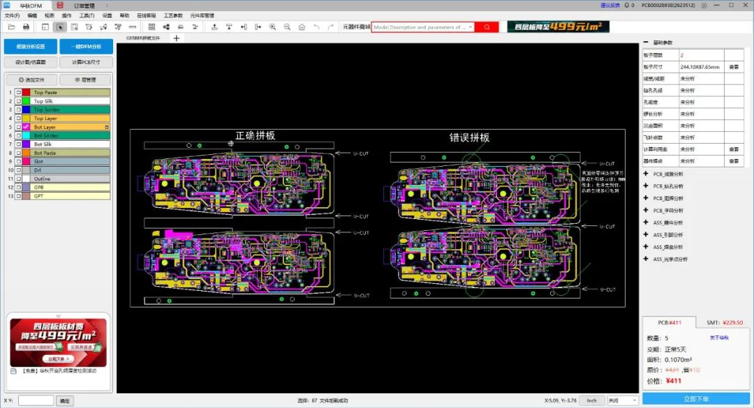
1) When using the V-scoring bridge connection method for panelization, if the outline of each unit is not completely flush, forced gapless panelization will create process dead zones, resulting in "dead sharp angles" that cannot be milled. A common remedial measure is adding drill holes to remove sharp angles, but this method is limited by the drill bit diameter, and after forming, a large amount of burrs and irregular protrusions will still remain (see right image). For this type of uneven V-scoring bridge connection, the optimized DFM solution is to artificially add breakaway tabs (process tabs). Extend a process redundancy at the connection position so that the milling cutter can mill directly into the inside of the breakaway tab along the outline during forming. In this way, even the smallest sharp angle positions can be thoroughly milled by the cutter, achieving smooth and burr-free outlines (see left image).
2) For complex irregular boards, full-line V-scoring panelization is usually not feasible. If forcibly panelized, the corners after outline routing will often leave tool joint burrs because the milling cutter cannot enter (see left image). For such scenarios, the most stable panelization method is using "mouse bite connections". By setting up mouse bite bridges in non-critical locations, combined with routed gaps, it can adapt to any complex geometric shape and ensure edge neatness after depanelization (see right image). Common Mistake: Forcing V-scoring on irregular board shapes instead of using mouse bites is a frequent error that inevitably results in poor edge quality and severe burrs.
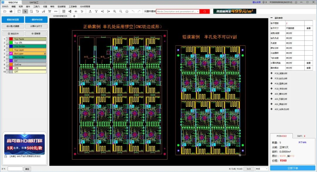
1) The panelization of castellated hole (half-hole) boards has a special characteristic: V-scoring must never be used at the castellated hole positions. This is because the V-shaped blade of the V-scoring generates lateral extrusion force during cutting, which directly cuts off or peels the copper plating inside the half-hole, resulting in holes with no copper or poor continuity. Therefore, a routed gap must be reserved at the castellated hole positions for special routing processing (see left image). Furthermore, if gapless panelization is used at castellated hole positions, the outer half of the holes will overlap into the interior of adjacent boards, causing the drilling process to directly scrap the adjacent boards (see right image). Common Mistake: Attempting to use V-scoring directly across castellated holes is a critical failure that destroys the copper plating and ruins the board's functionality.
2) For PCBs with castellated holes on three sides, "inverted panelization" logic is recommended. The reason is that sufficient routed space must be ensured on the half-hole side to protect the hole walls. Through inverted design, the castellated hole areas of two boards that require routing can be placed facing each other to centralize the routed gap, while the solid edges that do not require routing face outward to leave necessary panelization connection points (see left image). If the gapless panelization in the right image is referenced, it will cause half-hole failure, and the board cannot be properly formed.
3) For PCBs with castellated holes on all four sides, routed gaps must be reserved on all sides for routing processing. The engineering difficulty faced here is that the connection points are extremely small. If relying solely on board corner connections, "board breakage" is highly prone to occur during production handling or SMT pick-and-place. DFM recommends reinforcing the connections at the board corners, adding mouse bites if necessary; if the connection area is truly too small, consider omitting mouse bites, adopting full connections at the corners, and making special optimizations in the forming process.
1) In DFM inspections, the physical interference of board-edge components must be evaluated. When SMT components are installed extending beyond the PCB edge, gapless panelization must never be used. This is because the protruding part of the component will collide with the components or substrate of the adjacent board, resulting in an inability to mount. If breakaway tabs need to be added to the side with such board-edge components, the breakaway tabs must correspondingly be "hollowed out", otherwise the clearance space is insufficient, the components cannot be pressed down into place, and soldering failure will subsequently occur.
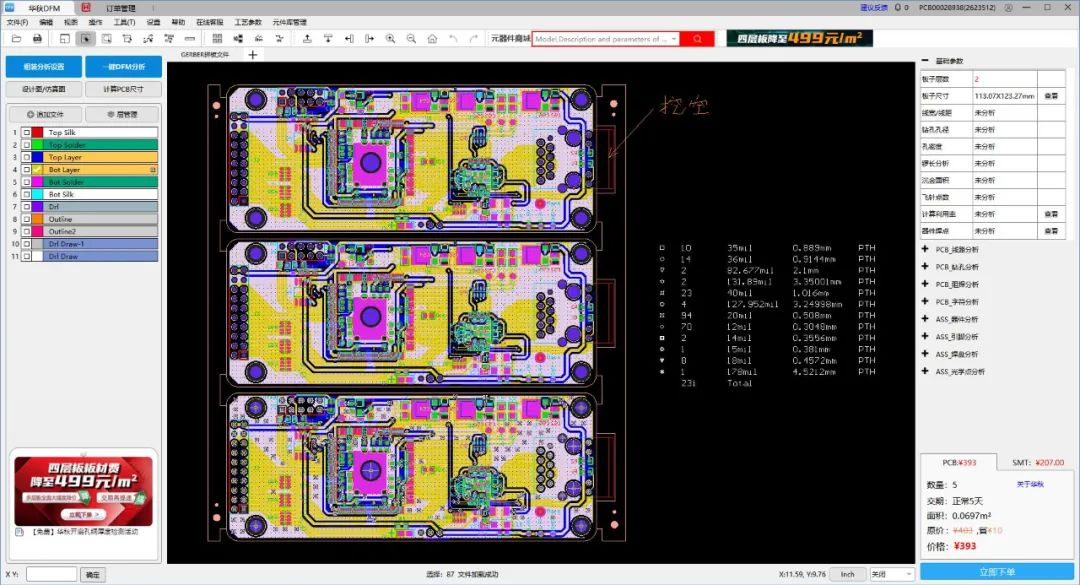
2) Regarding the situation where board-edge components extend beyond the board edge, another highly efficient solution is inverted panelization, rotating the side that extends beyond the board to face the outside of the panelization (see left image). In this way, during SMT assembly, the protruding components hang over the outside of the panelized array and will not interfere with other boards. If the protruding part is forcibly faced toward the inside of the panel, the substrate of the adjacent board will press against the components, causing production line halts or component damage (see right image). Common Mistake: Ignoring the outward protrusion of board-edge components and proceeding with standard panelization is a severe mistake that directly causes physical assembly interference.
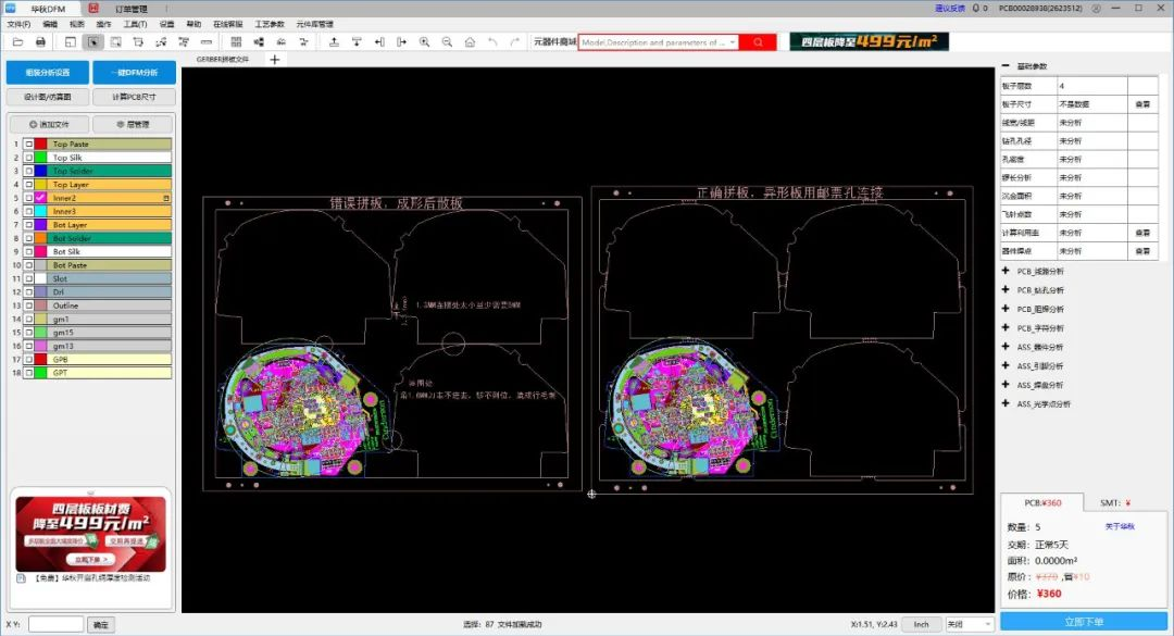
For circuit boards that cannot achieve straight-line V-scoring, such as irregular boards and circular boards, mouse bite bridge connections are the only mass production solution. The complex curves of irregular boards can only rely on CNC routing. For circular boards, if zero-gap V-scoring is attempted, the connection points will be extremely narrow, and uneven stress will easily cause board breakage; additionally, the separated circular edges will have burrs due to extrusion. When designing mouse bites, the hole diameter (usually 0.5mm-0.8mm) and center distance must be strictly controlled. If the mouse bite locations are spaced too far apart, it will lead to insufficient panel rigidity and board breakage; if the hole distance is too close, the connection material thickness is insufficient, which will also cause unexpected breakage during the production process. Common Mistake: Setting the distance between mouse bites too large or too small is a frequent oversight that directly compromises the structural integrity of the panel during SMT processing.
In certain complex designs, when parts of the outline are not flush and V-scoring connections must be used, because some areas are routed empty, the support strength of the overall panel framework will weaken, producing "wobbling" or "breaking" risks. In such DFM scenarios, mouse bite connections need to be additionally added in the routed gaps as reinforcing ribs to enhance the strength of the entire panel, preventing board breakage accidents during wave soldering or SMT rail transport.
Methodology First: A systematic approach is critical. Before finalizing any panelization, engineers must perform a comprehensive Design for Manufacturability (DFM) check. The absolute priority is to verify the board's outline shape, the appropriateness of the connection methods, clearance for board-edge components, and the risks associated with castellated holes. Once these fundamental aspects are confirmed, engineers should utilize professional DFM tools to double-check routed gaps, CNC tool paths, and potential assembly interference.
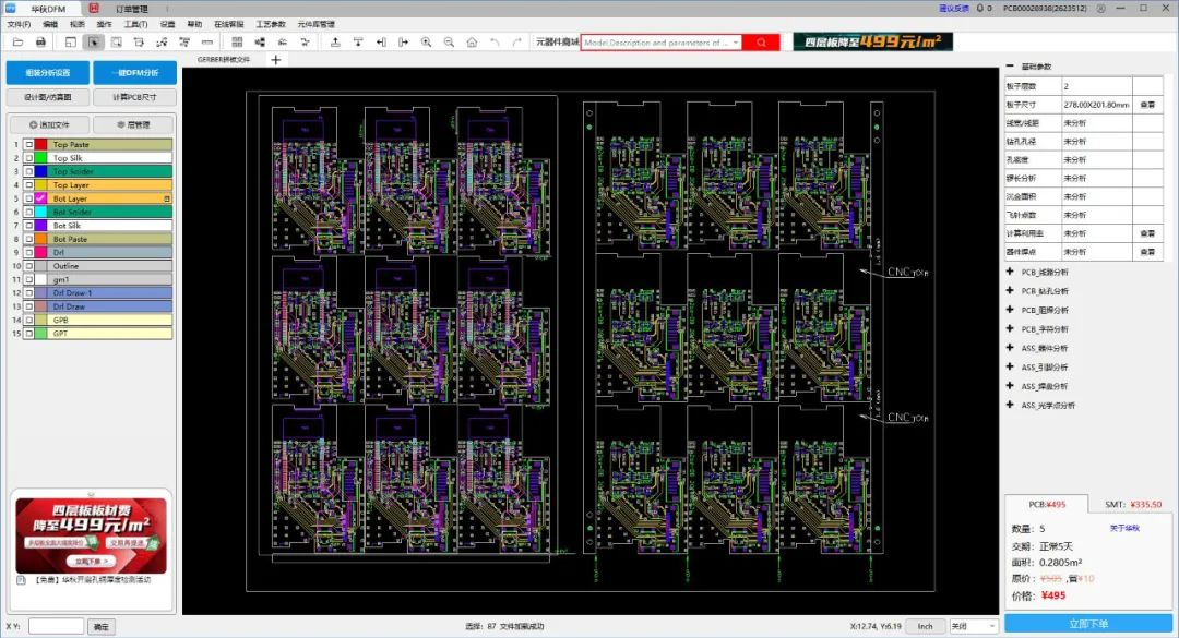
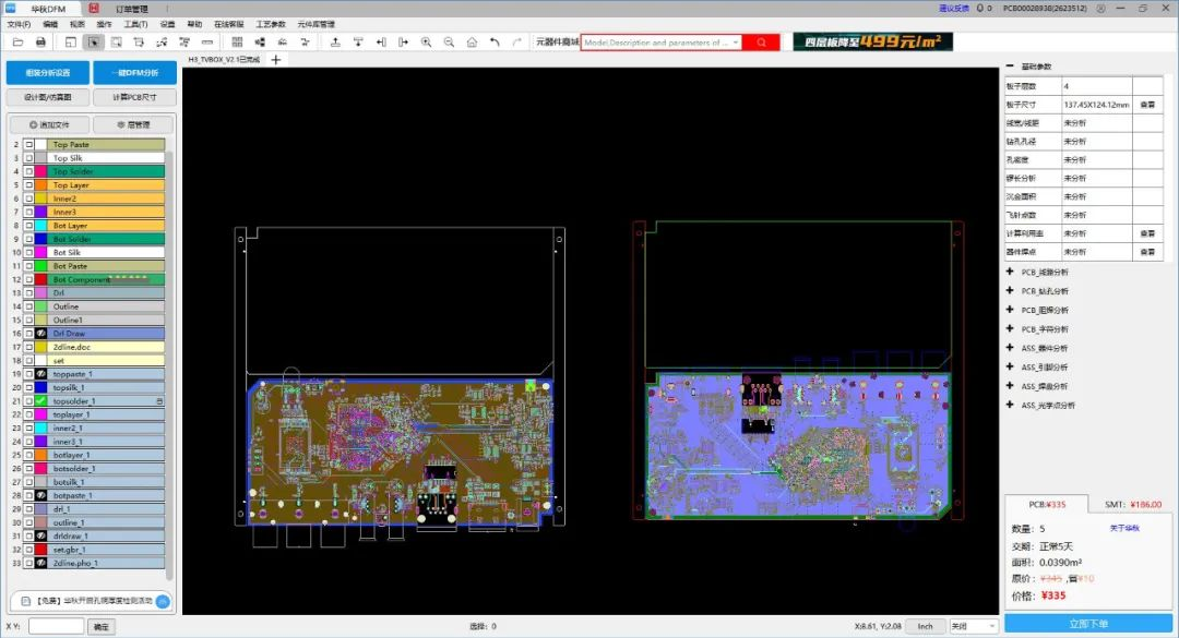
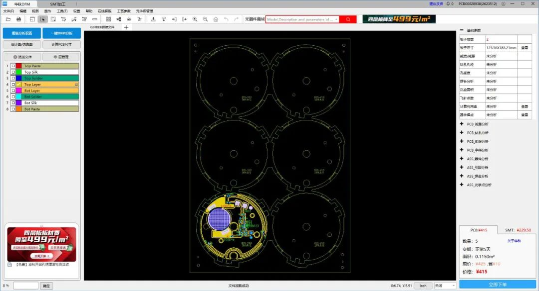
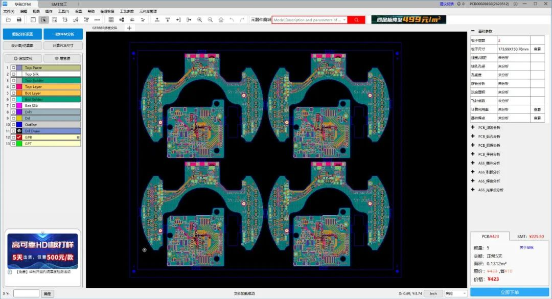
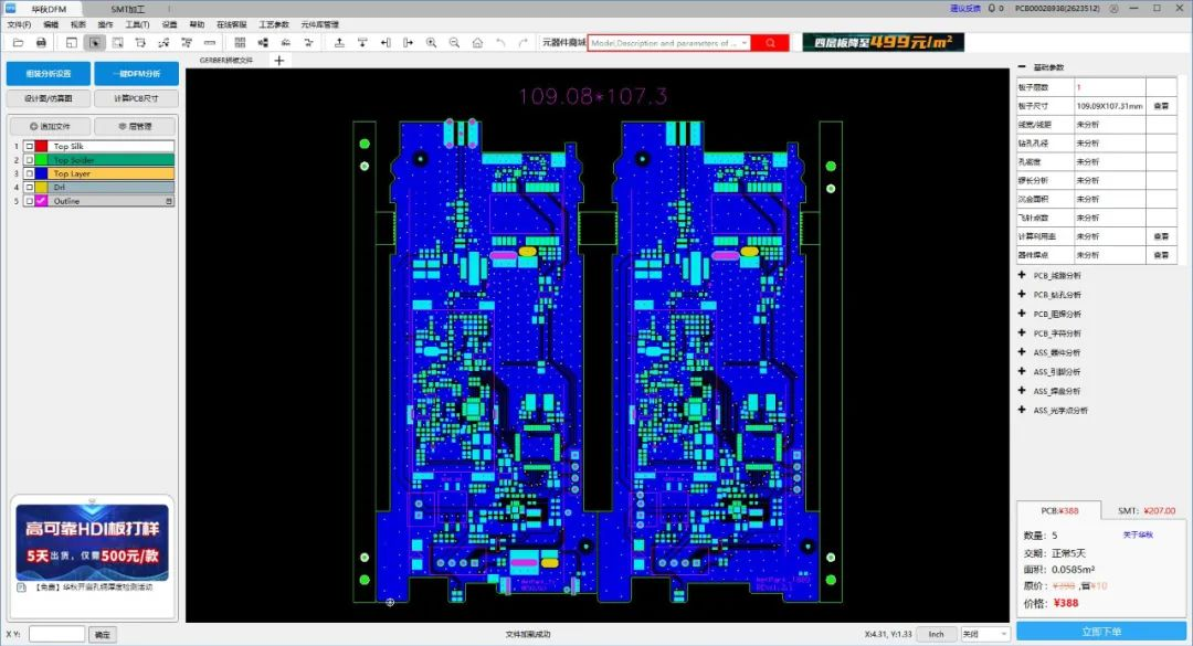
After designing the PCB and applying this methodology, deep analysis and inspection must be conducted to ensure subsequent smooth mass production. Here, we recommend a tool that can one-click smartly inspect PCB layout and process optimal solutions: HQDFM Software. Simply upload the PCB or Gerber file, click "One-Click DFM Analysis", and the system can automatically identify panelization risks and evaluate manufacturability based on real manufacturing process parameters.
HQDFM is a leading domestic PCB manufacturability and PCBA assembly analysis software, possessing over 3 million component libraries, which can significantly enhance assembly analysis efficiency. In terms of PCB bare board analysis, the software covers 19 major categories and 52 detailed inspection rules; for PCBA assembly analysis, it features 10 major categories and 234 detailed inspection rules.
This tool can accurately identify over 99% of potential manufacturing hidden dangers, helping design engineers predict risks before prototyping and production, meeting a variety of complex application scenarios. It not only significantly reduces product R&D iteration frequency and cost, but also provides functions such as one-click panelization calculation (maximizing board material utilization), smart impedance calculation, and component spatial interference inspection, avoiding production hidden dangers from the source and improving the mass production pass-through rate.
Still, need help? Contact Us: support@nextpcb.com
Need a PCB or PCBA quote? Quote now


 Surface

