
 NextPCB Capabilities
Printed Circuit Boards
NextPCB Capabilities
Printed Circuit Boards
 PCB Assembly
 Layer Buildup
 SMD-Stencils
 PCB Design-Aid & Layout
 Mechanics
 Quality
 Drills & Throughplating
 Factory & Certificate
 PCB Assembly Factory Show
Certificate
PCB Assembly Factory Show
Certificate
Support Team
Feedback:
support@nextpcb.com


Printed Circuit Board Assemblies (PCBA) are frequently exposed to harsh environments characterized by high humidity, salt spray, dust, and chemically corrosive gases. These external factors can lead to leakage currents, short circuits, and even electrochemical corrosion of metallic components. To guarantee the long-term operational stability of electronic equipment under such adverse conditions, applying a conformal coating (commonly known as "three-proof paint" in some regions) is a critical manufacturing process.
To ensure this protective layer genuinely fulfills its purpose, engineering teams must fully understand and implement strict pcb conformal coating quality requirements. This involves much more than simply applying material on the production line; it spans from initial material selection and equipment parameter tuning to post-process inspection and rework. Based on engineering practice, this article systematically outlines core standards, the root causes of common defects, and the technical pain points frequently encountered in actual manufacturing.
The ceiling of coating quality is largely determined by the physical and chemical properties of the materials selected during the early stages. In recent years, driven by environmental regulations such as RoHS and REACH limiting Volatile Organic Compounds (VOCs), and the push for higher Units Per Hour (UPH) in manufacturing, material selection has shifted significantly.
To help you choose the most suitable material while maintaining a balanced production line, the following table summarizes the core engineering characteristics of mainstream coatings:
| Resin Base (Type) | Process & Cure Speed | Reworkability | Mechanical Protection | Environmental Resistance* | Key Advantages & Engineering Notes |
|---|---|---|---|---|---|
| Acrylic (AR) | High / Fast | Excellent | Low | Fair | Easy to apply and rework with IPA; best for consumer electronics. |
| Polyurethane (UR) | Medium | Difficult | High | Excellent | Superior moisture and chemical resistance; ideal for automotive/industrial. |
| Epoxy (ER) | Medium / Slow | Extreme | Excellent | Excellent | Highest mechanical strength; prone to stress; used in high-vibration areas. |
| Silicone (SR) | Low / Slow | Fair | Low | Excellent | Outstanding thermal stability (-60°C to 200°C); flexible and low-stress. |
| UV Dual-Cure | Excellent | Medium | High | High | Fastest UPH; surface cures in seconds; secondary moisture cure for shadows. |
*Environmental Resistance includes moisture, salt spray, and chemical exposure.
Once material characteristics are defined, manufacturing must follow strict industry specifications to verify the final state of the coating.
Industry acceptance of coating quality primarily relies on two core international standards: IPC-CC-830 , which focuses on material property qualification, and IPC-A-610, which focuses on physical visual inspection.
Thickness is the most critical control variable in the coating process. IPC-CC-830 specifies recommended thickness ranges for different substrates. For example, acrylic and polyurethane are typically required to be between 25 μm and 75 μm, while silicone materials, due to their physical nature, allow a wider range, usually between 50 μm and 210 μm.
In practice, thickness readings must be obtained from a flat surface of the PCB that is free from component obstruction and where the coating is fully cured. Production lines typically use test coupons (of the same material as the main board) or metal/glass slides that travel through the oven with the assembly. Data is then collected using non-destructive equipment like eddy current thickness gauges to extrapolate the actual product's coating thickness.
According to IPC-A-610, a compliant coating must be transparent, uniformly distributed, and fully cured. No conductive foreign material is allowed to be embedded or entrapped in the minimum electrical clearance between bridging pads or adjacent conductive surfaces. Any deviation from these states is classified as a process defect.
Combined with microscopic visual inspection, here are several common coating defects and their engineering root causes:
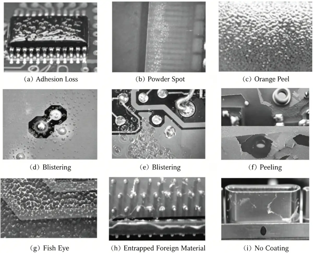
Common Visual Defects in PCB Conformal Coating
Even with a solid understanding of standards, engineers face complex physical and chemical challenges during mass production.
The Phenomenon: Low-viscosity coatings seep along microscopic gaps between masking tape and connector housings, penetrating deep into pins and causing contact failure.
Solution: Move beyond standard Kapton tape; use Peelable Solder Mask for a tighter seal at the base, or custom 3D-printed TPU boots for physical interference-fit protection.
The Phenomenon: Areas under BGA/QFP packages don't receive UV light and stay in a "liquid/gel" state. During later thermal cycling, this uncured monomer vaporizes, bursting the surface coating.
Solution: Enforce a 48–72 hour secondary moisture-cure period. Never pack boards in airtight bags immediately after UV processing.
The Phenomenon: Antennas shift center frequency or return loss spikes post-coating due to the change in dielectric environment (Dk shifts from 1 to ~3).
Solution: Proactive design is key. Include the coating as a dedicated dielectric layer in HFSS/ADS simulations during the layout stage for impedance compensation.
The Phenomenon: Over-spraying leads to "pooling" at component leads. Since coatings have a high CTE, they contract significantly in cold tests, literally tearing leads off pads.
Solution: Perform microsection analysis or use UV tracers to inspect coverage. Avoid thickness buildup at component corners through precise spray valve tuning.
The Phenomenon: Epoxies/Urethanes resist solvents; using strong strippers can dissolve the PCB's own solder mask or chip packaging.
Solution: Use localized thermal-mechanical methods. Heat the area to ~150°C to soften the resin, then peel with a Teflon probe. Use high-power fume extraction for any burn-through rework.
Achieving pcb conformal coating quality requirements is a systems engineering task. It requires collaboration between Hardware Layout (for RF compensation), Process Engineering (for masking/pathing), and Production Management (for cure control). Only through this cross-functional approach can coatings truly provide the long-term reliability required for mission-critical electronics.
For more information on matching strategies and process details, please refer to the NextPCB Blog: PCB Conformal Coating Applications.
For more information on matching strategies and process details, please refer to the NextPCB Blog: PCB Conformal Coating Applications.
Still, need help? Contact Us: support@nextpcb.com
Need a PCB or PCBA quote? Quote now


 Surface

