Contact Us
Blog >> Blog Details Page

How to Silkscreen PCB at Home

Posted:06:05 PM July 12, 2021 writer: louise

What is PCB silkscreen?


PCB Silkscreen is a layer of ink traces made use of to determine elements, examination factors, parts of the PCB, advising signs, logo designs as well as marks, and so on. This silkscreen is normally used on the element side; nevertheless making use of silkscreen on the solder side is additionally not unusual. Yet this might enhance the expense. Basically, a thorough PCB silkscreen can aid both the maker and also the designer to find as well as recognize all the elements.


PCB Silkscreen


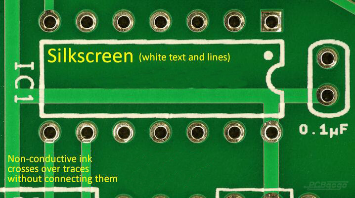
The ink is non-conductive epoxy ink. The ink utilized for these markings is extremely developed. The common shades we generally see are black, white as well as yellow. PCB software program additionally utilizes basic typefaces in silkscreen layers however you can pick various other typefaces from the system also. For standard silk screening, you need a polyester display extended on lightweight aluminum structures, a laser image plotter, a spray designer as well as healing stoves.


  Why Choose NEXTPCB Manufacturer  


DIY Silkscreen PCB Guidelines


  1. 1. Produce a layout making use of photo modifying programs such as Photoshop or CAD. You can additionally hand attract a layout as well as check it right into your computer system. Remember that the style ought to be really clear, with reasonably thick black lines and also dots. These photos are called traces.
  2. 2. Examination print your photo on a sheet of routine paper making use of a printer. Ensure to establish your printer for the darkest photo.
  3. 3. Cut the sides of the paper off the picture, leaving a little boundary.
  4. 4. Sand your PCB board in a cross-hatch pattern making use of 400 grit paper. Tidy the mess of the board making use of a typical cleaner such as scrubbing alcohol.
  5. 5. Iron your paper to the board. Make certain the iron is set on the highest possible temperature level which it has actually totally heated up. The ironing procedure needs to take in between 2 as well as 5 mins, relying on the dimension of your board. If you are uncertain if sufficient time has actually passed, provide the board an additional min of ironing. You ought to have the ability to see the traces with the paper.
  6. 6. Establish the board in a dish of warm water. This will certainly trigger the paper to divide from the board. It needs to take around 10 mins. You might need to hand draw the paper from the board.
  7. 7. Go down the board right into the ferric chloride option. Maintain a mindful watch on the remedy, making use of a plastic fork to check the board. This action must take around 10 to half an hour. This service gnaws the copper on the PCB board, leaving a clear pattern.
  8. 8. Eliminate the board from the service. Utilize the acetone printer toner as well as a Q-tip to eliminate any type of left-over copper.
Tag: PCB silkscreen
  • PCB
    Prototype
  • PCB
    Assembly
  • SMD
    Stencil

Dimensions: (mm)

×

Quantity: (pcs)

5
5
10
15
20
25
30
40
50
75
100
120
150
200
250
300
350
400
450
500
600
700
800
900
1000
1500
2000
2500
3000
3500
4000
4500
5000
5500
6000
6500
7000
7500
8000
9000
10000

Other Quantities:(quantity*length*width is greater than 10㎡)

OK

Layers:

Thickness:

Quote now