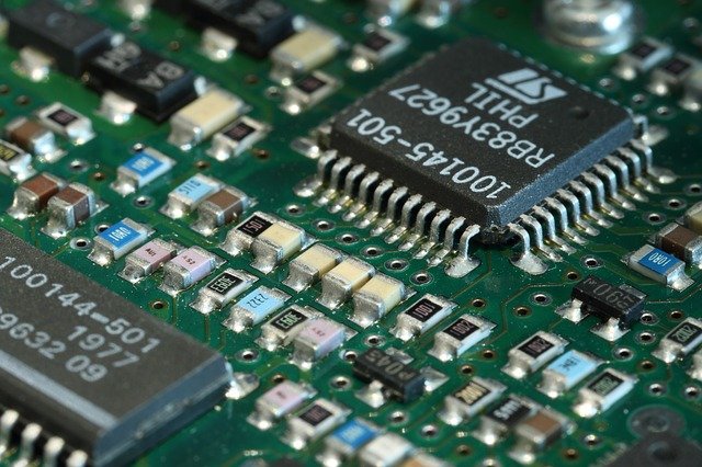
how to Get Rid Of a PCB Solder Mask Guidelines
Soldering electronic devices settings up can create numerous troubles, consisting of solder or change deposit build-up in undesirable areas on a published circuit card. A solder mask is a slim safety layer put on a published circuit card meant to manage this unintentional build-up as well as protect against undesirable solder links. Once in a while, solder masks will certainly require to be gotten rid of from a published circuit card in scenarios such as board production problems or circuit style modifications. This mask can be gotten rid of with one or a mix of these strategies: scratching and also fining sand, machining, chemical removing, or abrasion.
Scuffing and Fining Sand the Solder Mask
- 1.Scratch the solder mask layer far from the PCB thoroughly with the razor blade. Constantly put on shatterproof glass to stay clear of injury throughout this procedure.
- 2.Sand the PCB solder mask away with the mechanical eraser. This procedure calls for a high degree of ability to stay clear of damages to various other locations of the PCB.
- 3. Evaluate the PCB for unintended damages to the board itself or any kind of electric part traces.
Machining
- 4.Establish the carbide-tipped mill's idea to guarantee that just the PCB solder mask will certainly be impacted by the device's reducing idea. This is a rigorous dimension that might call for using a microscopic lens add-on.
- 5.Cut the PCB solder mask away with the carbide-tipped mill, staying clear of damages to various other electric traces or locations of the solder mask.
- 6.Check the PCB for unintended damages to the board itself or any type of electric part traces.
PCB Prototype Quote
Chemical Stripping
- 7.Shield the locations to be untouched with the concealing tape.
- 8.Use the industrial solder mask chemical cleaner with the brush just to the uncovered locations. Constantly use latex handwear covers for security.
- 9.Tidy the industrial solder mask chemical cleaner from the PCB with paper towels. The cleaner functions promptly and also should be eliminated prior to it harms undesirable locations.
- 10.Evaluate the PCB for unintended damages to the board itself or any type of electric part traces.
Abrasion
- 11.Safeguard any kind of location not to be influenced by abrasion with covering up tape.
- 12.Blast the solder mask away with the electronic device's micro blaster. Understand fixed electrical energy build-up throughout this procedure to stay clear of electrostatic discharge damages to any kind of elements.
- 13.Check the PCB for unintended damages to the board itself or any kind of electric part traces.

 NextPCB Capabilities
 PCB Assembly
 Layer Buildup
 SMD-Stencils
 PCB Design-Aid & Layout
 Mechanics
 Quality
 Drills & Throughplating
 Factory & Certificate
 PCB Assembly Factory Show
Certificate
PCB Assembly Factory Show
Certificate


 Surface

