
 NextPCB Capabilities
Printed Circuit Boards
NextPCB Capabilities
Printed Circuit Boards
 PCB Assembly
 Layer Buildup
 SMD-Stencils
 PCB Design-Aid & Layout
 Mechanics
 Quality
 Drills & Throughplating
 Factory & Certificate
 PCB Assembly Factory Show
Certificate
PCB Assembly Factory Show
Certificate
Support Team
Feedback:
support@nextpcb.com


Efficient Surface Mount Technology (SMT) assembly starts with the right PCB size and process edge design. When you design PCB size carefully, you enhance manufacturability and reduce production costs. For instance, poor component arrangement can disrupt assembly efficiency, while missing fiducial marks may lead to misaligned placements of parts like QFP or BGA. Components placed too close to the PCB edges can also hinder machine operations. By optimizing dimensions and adding process edges, you ensure stability during production, accurate component placement, and smoother workflows, all of which contribute to better performance and cost savings.
Surface Mount Technology (SMT) assembly is a highly efficient method for mounting electronic components onto printed circuit boards (PCBs). It eliminates the need for through-hole soldering by placing components directly on the PCB surface. This process is ideal for modern electronics, where compact designs and high-speed production are essential. SMT assembly works best when PCBs meet specific size and layout requirements. For example, the equipment used in SMT production relies on precise alignment and stability to ensure accurate component placement. A well-designed PCB size supports these requirements, reducing the risk of errors and improving manufacturing yield. Additionally, avoiding overcrowding of components is critical. Overcrowded layouts complicate assembly, increase the likelihood of errors, and lower production efficiency
The size of your PCB directly impacts its compatibility with SMT equipment. Machines like pick-and-place systems and reflow ovens have specific size constraints. If your PCB is too small, it may lack the stability needed for accurate component placement. Conversely, oversized PCBs may exceed the equipment's handling capacity, leading to production delays or additional costs.
For instance, many manufacturers require PCBs to be at least 60×60 mm for SMT assembly. Smaller designs often need to be panelized, where multiple PCBs are grouped together in a single panel. This approach improves mounting accuracy and ensures the board remains stable during production. Panelization also enhances thermal management and electrical performance, as larger areas dissipate heat more effectively and reduce signal interference.
Process edges, also known as panelization edges, play a vital role in ensuring smooth SMT production. These edges provide additional space around the PCB for handling, alignment, and stability during assembly. Without process edges, the PCB may shift or misalign, leading to errors in component placement.
A well-designed process edge offers several benefits:
| Aspect | Description |
| Quality Control | Ensures traceability, allowing quick identification of faulty components or process errors. |
| Regulatory Compliance | Provides documentation and audit trails to meet industry standards and regulations. |
By incorporating process edges into your PCB design, you enhance manufacturability and ensure compliance with industry standards. This
small addition can significantly improve the overall quality and efficiency of your SMT assembly process.
When designing PCB size for SMT assembly, you must consider the minimum and maximum dimensions that align with industry standards. These dimensions ensure compatibility with SMT equipment and maintain production efficiency. For example, most SMT machines require PCBs to be larger than 60×60 mm to ensure stability during the assembly process. Smaller PCBs often need to be panelized to meet these requirements.
The following table outlines common size specifications for PCBs in SMT applications:
| Specification | Minimum Value | Maximum Value |
| Minimum finished PCB size | ≥20mm | <10mm |
| Maximum finished board size | 10mm≤Size<20mm | 508×610mm(single/double) |
| Minimum board thickness(single/double) | ≥0.3mm | <2.00mm (14L) |
Ensuring your PCB falls within these ranges helps avoid production delays and additional costs. Larger PCBs also improve thermal management and electrical performance, which are critical for high-power designs.
Panelization is a technique where multiple smaller PCBs are grouped into a single panel for manufacturing. This approach enhances efficiency by allowing simultaneous processing of multiple boards. It also reduces material waste and improves consistency in assembly.
Here are some key benefits of panelization:
The following table highlights efficiency improvements from advanced panelization techniques:
| Efficiency Improvement | Description |
| Heightened Precision | Automation ensures accurate construction processes. |
| Improved Productivity | Simultaneous processing of multiple boards enhances productivity. |
| Minimized Waste | Reduces material waste during the manufacturing process. |
Additionally, panelization is particularly effective for small PCBs with irregular shapes. It reduces lead time, lowers labor costs, and facilitates quality control. By incorporating panelization into your design process, you can achieve significant cost savings and improved manufacturability.
Thermal and electrical performance are critical factors when you design PCB size for SMT assembly. Effective thermal management ensures the longevity and reliability of your PCB, especially in high-power applications. Components like power transistors generate significant heat, which must be dissipated to prevent damage to nearby parts.
Here are some tips to optimize thermal and electrical performance:
Even distribution of power across the PCB is also essential. Uneven power distribution can lead to overheating in specific areas, compromising the board's performance. By addressing these considerations, you can ensure your PCB operates efficiently and reliably under various conditions.
Process edges play a crucial role in ensuring smooth SMT assembly. These edges provide additional space around the PCB, enabling machines to handle, align, and stabilize the board during production. Without them, your PCB may shift or misalign, leading to errors in component placement and reduced manufacturing efficiency.
Here are some key benefits of incorporating process edges into your PCB design:
Tip: Always reserve enough space for process edges to ensure stability during transport and assembly. This small adjustment can significantly improve production efficiency and product quality.
When designing process edges, adhering to standardized dimensions ensures compatibility with SMT equipment and prevents production issues. These guidelines help you maintain proper spacing, alignment, and clearance for components and tooling.
| Feature | Recommended Dimension |
|---|---|
| Edge (Break-away tab) | Reserve more than 5mm at the side of the transport track; add about 5mm process edge if necessary. |
| Tooling Hole | Aperture usually 4mm; holes should be positioned 5mm from the sides and bottom, ensuring they support the PCB's center of gravity. |
| Component Clearance | No components should be within 3mm around the tooling holes. |
Additional guidelines for process edge design include:
By following these dimensions and placement rules, you ensure your PCB remains stable during assembly and avoids damage during depaneling.
Mistakes in process edge design can negatively impact SMT production efficiency. These errors often stem from improper spacing, alignment, or material choices. Identifying and addressing these issues early can save you time and resources.
| Error Type | Description | Potential Causes | Possible Solutions |
|---|---|---|---|
| Tombstoning | Component stands upright due to uneven solder forces. | Uneven heating, unequal heat sinks, insufficient solder paste force, misalignment. | Cover at least 50% of both pads, ensure high placement accuracy, maintain high preheat temperature. |
| Non-wetting or de-wetting | Solder does not adhere properly to components. | Poor PCB finish, excessive soaking time, insufficient heat during reflow. | Use better metal surface finishes, reduce profiling time, use proper flux. |
| Solder beading | Formation of solder balls near components. | Excessive solder paste, flux outgassing, excessive placement pressure. | Reduce stencil thickness, lower component placement pressure. |
| Insufficient fills | Inadequate solder paste deposited. | Blocked stencil aperture, insufficient squeegee pressure, high squeegee speed. | Segment large openings, clean stencil regularly, control squeegee speed. |
| Cold solder joint | Poor wetting leading to a grayish, porous appearance. | Insufficient heat, inadequate flux activation, impurities in solder solution. | Ensure maximum reflow temperature is adequate, avoid movement during reflow, check for contaminants. |
Note: Avoid placing components too close to the process edge. This can lead to alignment issues and damage during depaneling. Always ensure proper clearance for tooling holes and copper foil.
By addressing these common mistakes, you can optimize your process edge design and improve the overall efficiency of your SMT assembly.
Proper component placement is essential for efficient SMT assembly. It ensures smooth workflows, minimizes errors, and enhances the overall performance of your PCB. To optimize placement, follow these best practices:
By adhering to these guidelines, you create a design that supports efficient manufacturing and reduces the risk of costly errors.
The orientation of components directly impacts the performance and reliability of your PCB. Correct orientation improves signal integrity, reduces noise, and ensures efficient power distribution. The table below highlights how proper orientation affects different aspects of PCB performance:
| Aspect | Impact on Performance |
| Heightened Precision | Automation ensures accurate construction processes. |
| Improved Productivity | Simultaneous processing of multiple boards enhances productivity. |
| Minimized Waste | Reduces material waste during the manufacturing process. |
When designing your PCB, prioritize the orientation of high-speed components and power supplies. This approach ensures your board operates reliably under demanding conditions.
Placement conflicts and overlaps can disrupt SMT assembly and compromise the functionality of your PCB. To avoid these issues, follow these methods:
These practices help you design PCB size and layout that supports efficient assembly while maintaining high performance and reliability.
Aligning your PCB design with the capabilities of your manufacturer is essential for a successful production process. Manufacturers have specific technical limitations and strengths, which you must consider during the design phase. For instance, selecting a manufacturer with quality certifications like ISO 9001 or IPC-A-600 ensures adherence to high standards. These certifications reflect their commitment to delivering reliable and high-quality products.
Effective communication with your manufacturer also plays a crucial role. Discussing their equipment capabilities, material preferences, and design constraints early in the process can prevent costly revisions. Additionally, choosing a manufacturer with advanced technology and responsive support can significantly enhance your project's success. By aligning your design with their capabilities, you streamline production and reduce the risk of errors.
Adequate spacing and well-placed test points are critical for ensuring the manufacturability and testability of your PCB. Test points allow engineers to verify the functionality of your board during production. However, improper spacing can make these points inaccessible, leading to testing challenges.
The following table outlines key spacing guidelines for test points:
| Guideline Description | Details |
|---|---|
| Minimum Spacing Requirement | Test points must meet minimum spacing requirements for probe accessibility. |
| Clearance from Component Bodies | Maintain sufficient clearance from taller components to ensure accessibility. |
| Clearance from Board Edges | Position test points away from edges to avoid damage during testing. |
By adhering to these guidelines, you improve the accessibility of test points and ensure a smoother testing process. Proper spacing also prevents interference with other components, enhancing the overall reliability of your PCB.
Avoiding common DFM-related issues requires careful attention to detail during the design phase. Start by checking drill-to-copper spacing, especially as the number of holes increases. Proper spacing prevents short circuits and ensures signal integrity. Additionally, maintain regular board shapes to avoid cutting problems during manufacturing.
Here are some best practices to follow:
You should also avoid floating copper or solder mask slivers, as these can create shorts. Ensure sufficient annular ring sizes to prevent open circuits and keep copper away from board edges to avoid shorts in adjacent layers. By following these tips, you can design PCB size and layout that aligns with DFM principles, reducing production costs and improving quality.
Panelization is one of the most effective ways to optimize costs in PCB production. By grouping multiple PCBs onto a single panel, you can maximize material utilization and reduce per-unit costs. This approach also improves manufacturing efficiency by enabling simultaneous processing of multiple boards.
Several techniques can enhance panelization efficiency:
| Technique | Description | Benefits |
|---|---|---|
| V-scoring | Scoring the PCB material for easy separation. | Reduces material waste and improves efficiency. |
| Tab routing | Adding tabs on sensitive panel sides for easier handling. | Saves time and decreases waste. |
| Order Panelization | Consolidating multiple designs onto a single panel. | Minimizes production time and costs. |
| Combination Panelization | Combining various designs in one panel based on specific patterns. | Optimizes material use and reduces setup time. |
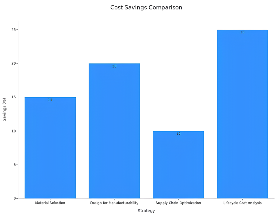
For example, using combination panelization allows you to fit different PCB designs into a single panel, reducing material waste and setup costs. Additionally, employing design software for panelization can cut setup costs by 10-25%. These techniques ensure you achieve cost savings without compromising quality.
Smart PCB design plays a crucial role in minimizing material waste. By adopting sustainable practices and innovative layouts, you can reduce excess material usage and improve production efficiency.
| Sustainable Practice | Contribution to Waste Reduction |
|---|---|
| Modular PCB Design | Reduces excess material through efficient layouts. |
| Renewable Resource Integration | Minimizes waste by using sustainable materials. |
| Energy-Efficient Fabrication | Lowers energy consumption, indirectly reducing waste. |
For instance, modular PCB design ensures that every inch of the board is utilized effectively, leaving minimal scrap material. Additionally, integrating renewable resources like biodegradable polymers into your design can further reduce environmental impact. Recycling-friendly layouts also support waste reduction by simplifying the recovery of valuable materials.
Balancing cost and performance in PCB layout requires careful consideration of design complexity and application requirements. While high-performance layouts may seem appealing, they often come with higher costs. Understanding the trade-offs between cost and functionality helps you make informed decisions.
| PCB Type | Complexity | Typical Cost per Square Inch (USD) | Typical Applications |
|---|---|---|---|
| Single-Layer | Lowest | $0.05 - $0.15 | Simple circuits, basic consumer electronics. |
| Double-Layer | Moderate | $0.10 - $0.30 | Intermediate complexity, IoT devices. |
| Multi-Layer (4-6 Layers) | High | $0.25 - $0.75 | Advanced industrial control, high-power electronics. |
| Multi-Layer (8+ Layers) | Very High | $0.60 - $2.00+ | High-speed digital, complex signal processing. |
For basic applications, single-layer or double-layer PCBs offer cost-effective solutions. However, for high-speed or power-intensive designs, multi-layer PCBs provide better performance despite their higher cost. To strike the right balance, evaluate your project's requirements and prioritize features that deliver the most value.
By optimizing your layout and leveraging efficient panelization techniques, you can design PCB size that meets both performance and budgetary goals.
Failing to account for SMT equipment requirements can lead to significant production inefficiencies. SMT machines have specific size constraints, and ignoring these can result in misaligned components or unstable boards during assembly. For example, if your PCB is smaller than 60×60 mm, it may lack the stability needed for accurate placement. This often necessitates panelization, which adds complexity and costs to the manufacturing process.
You should also ensure that the physical dimensions of components match their footprints on the PCB. Mismatched dimensions can cause incorrect placement, affecting the board's functionality. Missing component orientation or pin markings further complicates assembly, increasing the likelihood of errors. These issues not only disrupt production but also compromise the reliability of the final product.
To avoid these problems, always verify that your PCB design aligns with the capabilities of the SMT equipment. This includes checking size specifications, component footprints, and orientation guidelines. By doing so, you ensure smoother workflows and higher manufacturing yields.
Neglecting process edge specifications can severely impact the efficiency and quality of SMT assembly. Process edges provide essential support for handling, alignment, and stability during production. Without them, your PCB may shift or misalign, leading to errors in component placement.
Proper process edge design also ensures compliance with industry standards. For instance, reserving at least 5 mm for process edges helps maintain stability during transport and assembly. Missing fiducial marks or tooling holes can disrupt alignment, causing delays and increasing costs. Additionally, inadequate clearance around tooling holes can lead to damage during depaneling.
| Metric Type | Description |
|---|---|
| Quantity Metrics | Measures EDGE data amounts relative to baseline enrollment and claims reported through a separate form. |
| Quality Metrics | Assesses consistency of EDGE data against prior-year submissions or current-year ACA market data. |
| Error Resolution | Highlights the importance of data integrity and the financial impact of lost risk adjustment values due to data errors. |
By adhering to standardized dimensions and placement guidelines, you enhance manufacturability and reduce the risk of costly errors. This small adjustment can significantly improve production efficiency and product quality.
Poor panelization can disrupt the entire manufacturing process. Effective panelization arranges multiple boards into a single panel, optimizing manufacturing capacity and reducing waste. When panelization is poorly executed, it increases material waste and production costs, undermining the efficiency of SMT assembly.
For instance, irregular panel shapes or inconsistent spacing between boards can complicate handling and assembly. This often results in higher labor costs and longer lead times. Additionally, poor panelization can affect thermal management, leading to overheating issues that compromise the reliability of your PCB.
To avoid these consequences, focus on designing panels that maximize material utilization and streamline production. Techniques like V-scoring and tab routing simplify separation while minimizing waste. By prioritizing efficient panelization, you not only reduce costs but also improve the overall quality of your PCB design.
Designing PCB size and process edges thoughtfully is essential for achieving efficient SMT assembly. By following best practices, you ensure smoother workflows, reduce production costs, and enhance overall product quality. Proper component orientation and spacing prevent soldering issues, while grouping SMT components maximizes space utilization. These strategies also improve accessibility for hand-soldered parts and minimize rework. When you align your design with DFM principles, you create a cost-effective and reliable PCB that meets manufacturing standards.
PCB size affects equipment compatibility, stability, and production efficiency. A properly sized PCB ensures accurate component placement, better thermal management, and reduced signal interference. It also aligns with SMT equipment requirements, minimizing errors and delays during manufacturing.
Most SMT manufacturers recommend a minimum PCB size of 60×60 mm. Smaller PCBs require panelization to meet this standard. This ensures stability during assembly and improves mounting accuracy.
Process edges are additional spaces around the PCB. They provide stability during transport and assembly. They also include fiducial marks for alignment and simplify depaneling, ensuring smooth production workflows.
Panelization groups multiple PCBs into one panel. This allows simultaneous processing, reduces material waste, and improves consistency. It also simplifies handling and enhances productivity, especially for small or irregularly shaped PCBs.
Fiducial marks are reference points for SMT machines. They help align the PCB accurately during component placement. Place them on the process edges or corners of the PCB for optimal alignment.
Distribute heat-generating components evenly. Use wider ground lines and thicker metal foils. Add heatsinks or cooling solutions for high-power components. These steps prevent overheating and improve reliability.
Common mistakes include insufficient edge width, missing fiducial marks, and improper tooling hole placement. These errors can cause misalignment, damage during depaneling, or production delays. Always follow standard guidelines for process edge design.
Proper placement ensures smooth workflows and reduces errors. Align components consistently, maintain adequate spacing, and avoid placing parts too close to the PCB edge. These practices improve manufacturability and prevent soldering issues.
Still, need help? Contact Us: support@nextpcb.com
Need a PCB or PCBA quote? Quote now


 Surface

