
 NextPCB Capabilities
Printed Circuit Boards
NextPCB Capabilities
Printed Circuit Boards
 PCB Assembly
 Layer Buildup
 SMD-Stencils
 PCB Design-Aid & Layout
 Mechanics
 Quality
 Drills & Throughplating
 Factory & Certificate
 PCB Assembly Factory Show
Certificate
PCB Assembly Factory Show
Certificate
Support Team
Feedback:
support@nextpcb.com


Whether the overall structure of the board meets the production requirements, whether it can meet the mass production conditions of the board factory, and whether the production cost can meet the project budget.
These questions are full of question marks for most engineers, and it is generally easy to be incompletely considered in the design of the board.
Faced with the EQ inquiry feedback from the board factory, it was impossible to answer accurately, which caused the finished board to be scrapped and unable to be used. In the end, it was natural that the engineer had to carry it out.
How to standardize these "PCB inspection items" together for automatic inspection? Looking at the professional DFM software on the market:
Budget?
With hundreds of thousands at every turn, it is suitable for large companies that require high-intensity PCB reviews. As long as they are completed quickly and easily, the budget is not a problem. But for small companies with few PCB products and rapid changes, this price-performance ratio can only be prohibitive
Copyright?
The use of piracy is very likely to cause copyright risks
Compatibility?
Often can only detect fixed format files
This has caused problems with the current boards in the industry, and then frequently asked engineers to back up the situation.
So is there a free DFM software, even if the functions are not as strong as professional DFM software, but the basic functions can meet the review requirements of ordinary company PCB, efficient and free? ?
The answer is: YES!
Connect the design and production chain, so that the energy efficiency and quality control of the project/team can be doubled.
In order to help PCB engineers solve the ills of this industry, I refuse to go back. Today I will recommend a free and highly compatible PCB design analysis tool [NEXTDFM].
According to the actual measurement by a group of senior PCB engineers, it has the following practical functions.
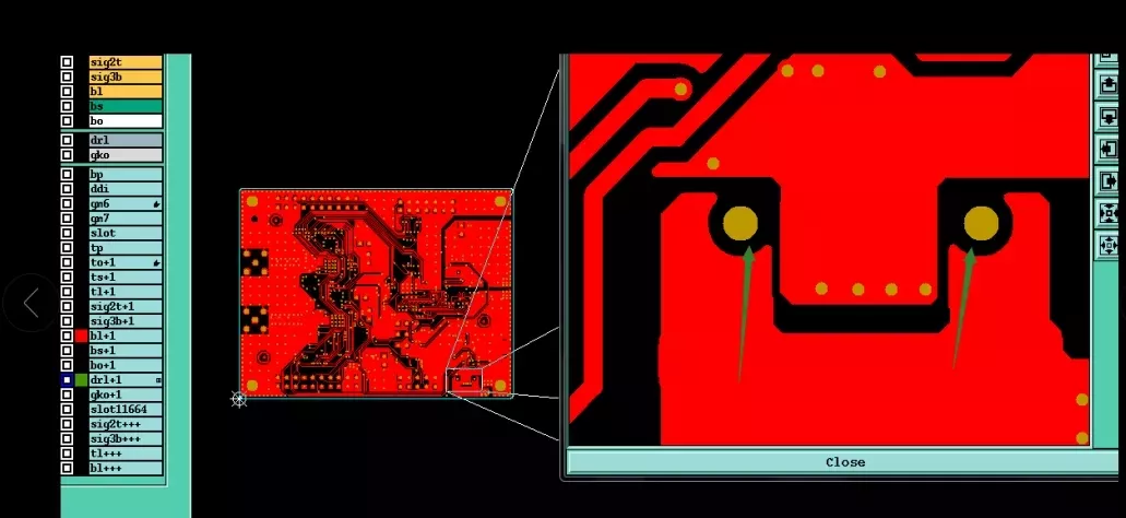
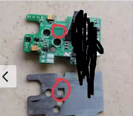
It can simulate the effect of the real object, and the specific performance is as shown in the figure below. Is this very close to the real object? Like some problems with no drilling, you can see it at a glance. If there is no rou file, then the hole position can be seen to be blocked.
More than 20 problems such as open and short circuit, minimum line width, line distance, etc., can be accurately located to the specific location
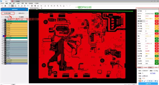
As shown in the figure below, on the right is a general result of its analysis. You can click to view the detailed content to help us judge whether there is a problem.
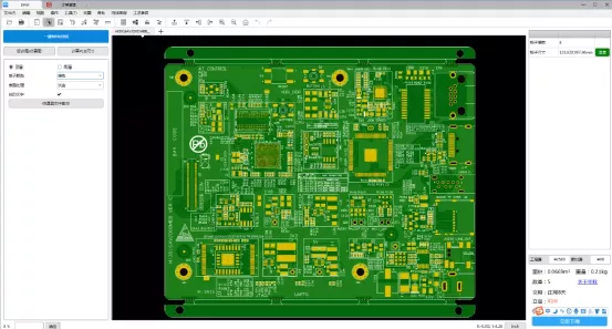
It can directly import PCB source files or Gerber files for analysis. There is no need to import Gerber files for analysis every time. It can support the import of PCB source files, including common software such as Allegro, Pads, and AD.
You can export Gerber files, coordinate files, and silk screen pdf files with one click.
More NEXTDFM functions
In addition, through my careful research, I also summarized the following very useful functions:
1. Warn items that affect prices, and give optimization plans for hidden dangers and items that affect prices
2. Multi-layer boards automatically match the laminated structure
3. Intelligent impedance tools, combined with production factors, calculate impedance data or reverse calculations.
4. Personalized jigsaw puzzle, seckill rule board or special-shaped board, stamp hole can be added.
Through the above functions, basically achieve the purpose of one-click analysis of the problem. The Xiaobai impedance calculation can also facilitate us to check the EQ inquiries of various board manufacturers. It is a tool worth recommending~ It can be said that the Prepare Artifacts]
Still, need help? Contact Us: support@nextpcb.com
Need a PCB or PCBA quote? Quote now


 Surface

