
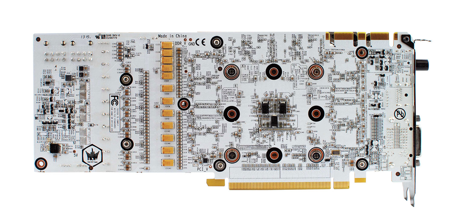
 NextPCB Capabilities
Printed Circuit Boards
NextPCB Capabilities
Printed Circuit Boards
 PCB Assembly
 Layer Buildup
 SMD-Stencils
 PCB Design-Aid & Layout
 Mechanics
 Quality
 Drills & Throughplating
 Factory & Certificate
 PCB Assembly Factory Show
Certificate
PCB Assembly Factory Show
Certificate
Support Team
Feedback:
support@nextpcb.com


White solder mask is a type of material that is used in printed circuit board (PCB) fabrication. Adding a polymer layer to PCB surfaces shields copper traces and pads from oxidation, moisture, and other environmental factors. The purpose of the solder mask is to prevent solder from sticking to areas where it is not intended to be, ensuring that electrical connections are made only where they are supposed to be.
White solder mask is so named because of its color, which is typically a bright white or cream color. This color is chosen because it provides high contrast against the green or blue solder mask commonly used in PCB manufacturing, making it easier for technicians to inspect the board for defects.
In this article,
The first step in the process of applying a white solder mask is to clean the PCB. Typically, people clean by using a solvent such as isopropyl alcohol that quickly evaporates and leaves no residue.
After cleaning the PCB, you can apply the white solder mask.
Typically, one applies the mask by screen-printing it onto the board through a stencil. To accomplish this, one places the stencil over the board and uses a squeegee to apply the mask. We then use a heat source such as an oven or a UV lamp to dry the mask.
After the mask has been applied and dried, it needs to be cured. We do this to ensure that the mask fully cures and does not crack or peel over time. The curing process requires heating the mask for a set time, based on the mask type and temperature.
Once the mask has been cured, the stencil is removed from the board. The user peels the stencil away from the board, leaving the white solder mask in place. Then, the inspector examines the board for any defects or imperfections in the mask and corrects them using touch-up methods if needed.
The screen printing machine is used to apply the white solder mask to the PCB. The machine utilizes the stencil to apply the mask, which then dries and cures, creating a protective layer on the board.
The lamp emits UV light, which causes the mask to harden and become more durable. PCB manufacturers can use UV lamps to apply white solder masks and other types of coatings, which showcases their versatility in the manufacturing process.
We use the oven to cure it, after applying and drying it. The oven exposes the mask to heat for a specific amount of time, depending on the type of mask and the curing temperature. This ensures the mask undergoes full curing and will not crack or peel over time.
In conclusion, NextPCB offers high-quality services that are cost-effective, making it an ideal choice for businesses of all sizes.
Additionally, our cutting-edge technology and state-of-the-art manufacturing processes guarantee precision and efficiency in every production run. Furthermore, our skilled and experienced team of engineers and technicians ensure that every detail is accounted for, from design to delivery. Consequently, our customers receive excellent quality PCBs that meet or exceed industry standards, all at a cost-effective price point. In conclusion, trust NextPCB for all your needs and experience top-notch service and quality every time.
Still, need help? Contact Us: support@nextpcb.com
Need a PCB or PCBA quote? Quote now


 Surface

