
 NextPCB Capabilities
Printed Circuit Boards
NextPCB Capabilities
Printed Circuit Boards
 PCB Assembly
 Layer Buildup
 SMD-Stencils
 PCB Design-Aid & Layout
 Mechanics
 Quality
 Drills & Throughplating
 Factory & Certificate
 PCB Assembly Factory Show
Certificate
PCB Assembly Factory Show
Certificate

Support Team
Feedback:
support@nextpcb.com


As electronic devices become faster and more compact, controlling electromagnetic interference has become one of the most important challenges in PCB design. High-speed processors, switching power supplies, and dense circuit layouts can generate unwanted electromagnetic noise that affects signal integrity and overall system performance. If not properly managed, this noise can lead to malfunctioning devices, communication errors, or failure to meet regulatory standards.
Two key concepts related to this issue are Electromagnetic Interference (EMI) and Electromagnetic Compatibility (EMC). EMI refers to unwanted electromagnetic energy that disrupts the normal operation of electronic systems, while EMC refers to the ability of a device to operate correctly in its electromagnetic environment without causing interference to other devices.
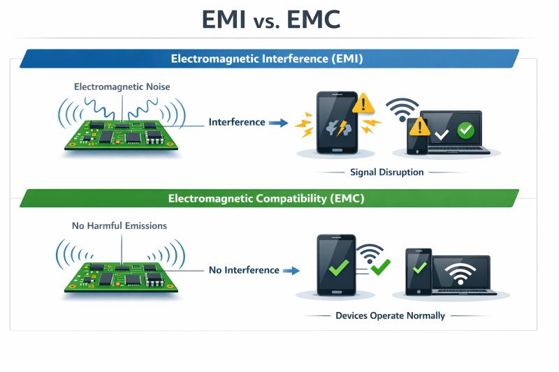
Comparison between EMI and EMC in PCB design showing interference effects vs proper electromagnetic compatibility
Modern products such as smartphones, IoT devices, automotive electronics, and industrial control systems must comply with strict electromagnetic compatibility standards such as FCC, CE, and CISPR. Poor PCB layout practices—such as improper grounding, long signal loops, or insufficient decoupling—can significantly increase EMI emissions.
Therefore, EMI and EMC considerations must be integrated early in the PCB design process. By applying proper stackup design, grounding techniques, routing strategies, and filtering methods, engineers can significantly reduce electromagnetic interference and ensure reliable system operation.
To design reliable electronic systems, it is important to clearly understand the difference between EMI and EMC and how they affect PCB performance.
Electromagnetic Interference refers to unwanted electromagnetic energy generated by electronic circuits that can disturb nearby devices or even other parts of the same system. In PCBs, EMI is commonly produced by fast switching signals, high-frequency clocks, power converters, and long signal traces that act as antennas.
EMI generally occurs in two main forms:
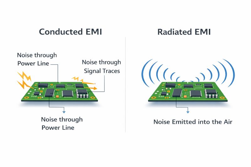
Types of EMI in PCB design: conducted EMI through circuits and radiated EMI emitted into the air
Conducted EMI: Conducted EMI travels through physical conductors such as power lines, ground connections, or signal traces. Noise generated by switching regulators or digital circuits can propagate through these paths and affect other components in the system.
Radiated EMI: Radiated EMI occurs when electromagnetic energy is emitted into the air from PCB traces, cables, or components. High-speed signals with large loop areas can behave like antennas and radiate electromagnetic waves that interfere with nearby electronic devices.
Electromagnetic Compatibility refers to the ability of an electronic device to function correctly in its electromagnetic environment without generating excessive interference for other devices. A PCB design with good EMC performance minimizes both the emission of electromagnetic noise and its susceptibility to external interference.
Achieving good EMC requires careful attention to several design factors, including PCB stackup structure, grounding strategy, signal routing, decoupling techniques, and component placement.
The PCB stackup plays a key role in controlling EMI by reducing radiation and improving signal integrity. Signals always return through a reference plane (typically ground), and any interruption in this path increases loop area and EMI.
To minimize interference, signal layers should be placed close to continuous reference planes, ensuring a controlled return path. For high-speed designs, multilayer PCBs (4-layer or 6-layer) are preferred as they provide dedicated ground and power planes for better EMI control.
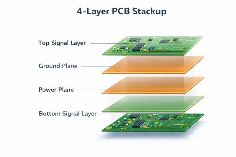
Typical 4-layer PCB stackup structure used for improving EMI control and signal integrity
A common and effective 4-layer PCB stackup looks like this:
Layer 1 – Signal (Top Layer)
Used for component placement and signal routing.
Layer 2 – Ground Plane
A continuous ground plane that provides a stable reference and return path for signals.
Layer 3 – Power Plane
Used for distributing power to different components.
Layer 4 – Signal (Bottom Layer)
Used for additional routing and lower-speed signals.
Placing the ground plane directly below the top signal layer helps reduce loop area and suppress EMI, while continuous planes also act as shields that prevent electromagnetic radiation from spreading across the board. Additionally, maintaining a symmetrical stackup and ensuring signal layers are adjacent to reference planes is essential, as poor design choices—such as routing high-speed signals between two signal layers without a reference plane—can significantly increase electromagnetic emissions.
Grounding is essential for controlling EMI, as it provides a low-impedance return path and prevents noise from spreading across the PCB. A solid ground plane is highly recommended because it ensures stable return currents and reduces electromagnetic radiation.
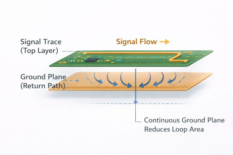
Continuous ground plane ensures proper return path and minimizes loop area to reduce EMI
Maintaining continuous return paths is critical—any interruption increases loop area and EMI. In mixed-signal designs, analog and digital grounds may be separated but should be connected at a single point. Additionally, ground stitching vias help maintain continuity across layers and improve shielding.
Poor routing practices can turn PCB traces into unintended antennas that radiate electromagnetic energy. By following proper routing guidelines, designers can significantly reduce EMI and improve signal integrity.
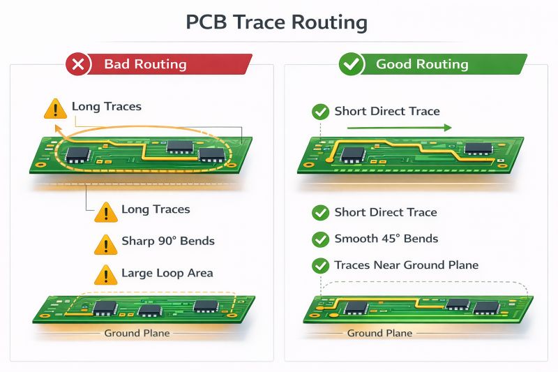
Good vs bad PCB trace routing practices for reducing EMI and improving signal integrity
| Practice | Benefit |
|---|---|
| Short, direct traces | Reduces loop area and EMI |
| Smooth bends (45°) | Avoids impedance discontinuities |
| Controlled impedance | Prevents reflections and noise |
| Differential routing | Cancels electromagnetic radiation |
| Close to ground plane | Ensures proper return path |
| Small loop areas | Minimizes radiation |
Noise in the power distribution network is a common source of EMI in electronic systems. Rapid switching of digital circuits can cause sudden current demands, which create voltage fluctuations and noise on the power lines. Without proper decoupling, this noise can spread across the PCB and affect other components.
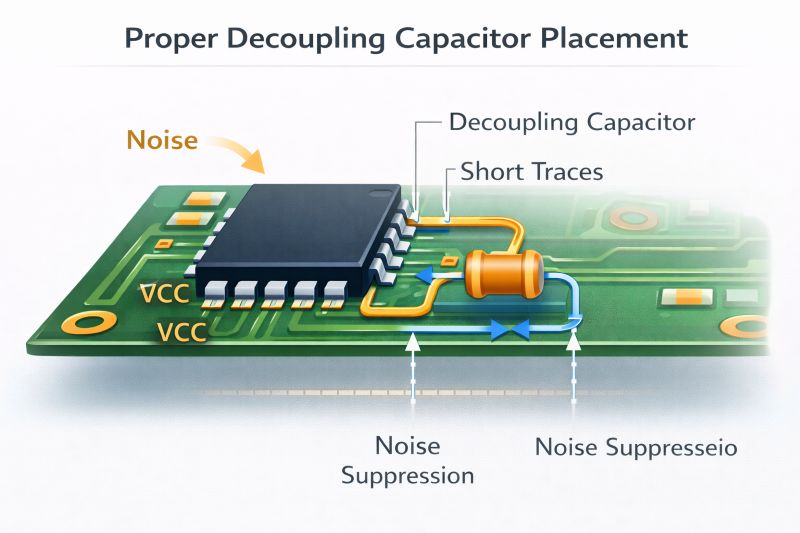
Correct placement of decoupling capacitors to reduce power noise and improve EMC performance
Decoupling capacitors are widely used to stabilize the power supply and suppress high-frequency noise. These capacitors act as local energy storage devices that quickly supply current to integrated circuits during switching events. By providing a short path for transient currents, decoupling capacitors prevent noise from propagating through the power network.
For effective decoupling, capacitors should be placed as close as possible to the power pins of integrated circuits. The distance between the capacitor and the IC should be minimized to reduce inductance in the current path.
Designers often use multiple capacitor values to handle different noise frequencies. For example:
0.1 µF capacitors are commonly used for high-frequency noise suppression.
1 µF to 10 µF capacitors help stabilize lower-frequency power fluctuations.
Another important factor is designing an efficient Power Distribution Network (PDN). A good PDN includes wide power traces or dedicated power planes, short current paths, and proper decoupling capacitor placement. Using power planes instead of narrow traces reduces impedance and improves power stability.
By implementing proper decoupling strategies and designing a stable power distribution network, PCB designers can significantly reduce power-related noise and improve overall EMC performance.
In many cases, proper PCB layout and grounding can significantly reduce EMI. However, in high-frequency or high-power designs, additional techniques such as shielding and filtering may be required to further suppress electromagnetic noise.
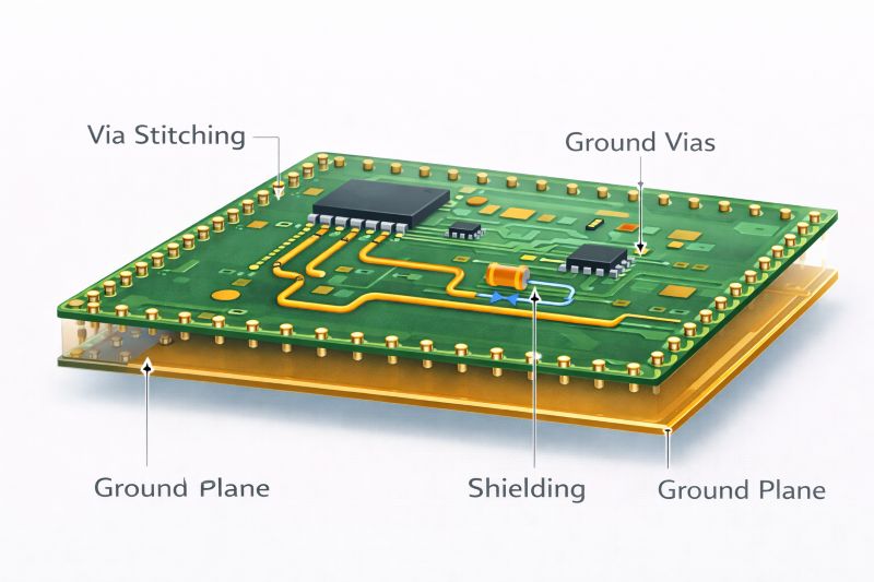
Via stitching technique used to maintain ground continuity and reduce electromagnetic interference
Shielding is used to prevent electromagnetic radiation from entering or leaving a specific area of the circuit. One common approach is the use of metal shielding cans, which are placed over sensitive or noisy components. These shields act as barriers that contain electromagnetic fields and prevent interference with nearby circuits.
Another useful technique is adding ground shielding traces around high-speed or sensitive signal lines. These grounded traces help contain electromagnetic fields and reduce radiation from the signal path.
Filtering components are also widely used to suppress unwanted noise. For example:
Ferrite beads are commonly placed in power lines to block high-frequency noise while allowing DC current to pass.
EMI filters can be used at power input stages to prevent noise from entering or leaving the device.
Common-mode chokes are often used in communication interfaces such as USB, Ethernet, and HDMI to reduce common-mode noise.
These filtering components work by attenuating unwanted high-frequency signals before they can propagate through the circuit or radiate into the surrounding environment.
When used together with proper layout practices, shielding and filtering techniques provide an additional layer of EMI protection, especially in complex or high-speed electronic systems.
Via stitching is a widely used technique in PCB design to improve grounding and reduce electromagnetic interference. Stitching vias connect ground planes across different PCB layers, helping maintain a continuous low-impedance path for return currents.
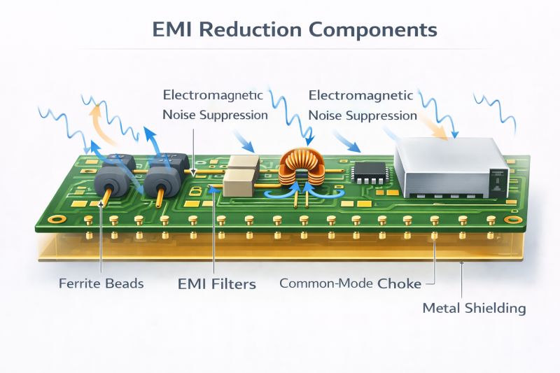
Common components used for EMI suppression in PCB design such as ferrite beads and EMI filters
Even with careful design practices, EMI issues may still arise during product development, making testing an essential step to ensure compliance with EMC requirements and regulatory standards. Many engineers perform pre-compliance testing in the early stages to identify potential problems before final certification, saving both time and cost. These tests are typically conducted using tools such as spectrum analyzers, near-field probes, and small anechoic chambers.
For official certification, products must pass standardized EMC tests defined by regulatory organizations. Some commonly used standards include:
During these tests, engineers measure both radiated emissions and conducted emissions to ensure that the device does not produce excessive electromagnetic interference. If a product fails EMC testing, designers may need to modify the PCB layout, improve shielding, add filtering components, or adjust grounding strategies.
By combining good PCB design practices with proper testing procedures, engineers can ensure that their products meet EMC regulations and operate reliably in real-world environments.
| Category | Common Mistakes | Recommended Fix |
|---|---|---|
| Grounding | Split or fragmented ground planes, interrupted return paths, floating ground areas | Use a solid, continuous ground plane and ensure clear return paths |
| Trace Routing | Long high-speed traces, large loop areas, 90° bends, poor differential routing | Keep traces short, direct, and close to reference planes with smooth routing |
| Decoupling & Power | Missing capacitors, poor placement, single capacitor value, weak PDN design | Use multiple decoupling capacitors near IC power pins and design a low-impedance PDN |
| Stackup Design | No ground plane, improper layer arrangement, signal layers without reference planes | Use a proper multilayer stackup with signal layers adjacent to ground planes |
| Component Placement | Noisy components near sensitive circuits, large current loops, poor grouping | Separate analog, digital, and power sections and minimize loop areas |
| Shielding & Filtering | Missing EMI filters, ferrite beads, shielding, or common-mode chokes | Use filtering components and shielding techniques where required |
| Via & Return Path | Insufficient stitching vias, broken return paths, poor via placement | Add ground stitching vias and maintain continuous return paths |
| Circuit Separation | Mixing analog, digital, and power circuits, shared noisy return paths | Maintain clear circuit separation and controlled grounding |
| Design Approach | Ignoring EMI during design, no pre-compliance testing | Consider EMI from the early design stage and validate with testing |
In conclusion, Electromagnetic interference remains a major challenge in modern PCB design as devices become faster and more densely integrated, making effective EMI control essential for reliable performance and regulatory compliance. Issues such as signal degradation and system malfunction often arise from poor design practices, but they can be significantly mitigated through a well-planned PCB stackup, solid grounding, optimized trace routing, and proper decoupling. Additional techniques like shielding, filtering, and via stitching further strengthen EMC performance. Most importantly, addressing EMI considerations early in the design phase—especially during layout and component placement—ensures more efficient and cost-effective solutions. By applying these proven EMI and EMC reduction strategies, engineers can develop robust, high-performance electronic systems that operate reliably in complex electromagnetic environments.
Still, need help? Contact Us: support@nextpcb.com
Need a PCB or PCBA quote? Quote now




