
 NextPCB Capabilities
Printed Circuit Boards
NextPCB Capabilities
Printed Circuit Boards
 PCB Assembly
 Layer Buildup
 SMD-Stencils
 PCB Design-Aid & Layout
 Mechanics
 Quality
 Drills & Throughplating
 Factory & Certificate
 PCB Assembly Factory Show
Certificate
PCB Assembly Factory Show
Certificate
Support Team
Feedback:
support@nextpcb.com


Altium Developer makes use of the layout to develop a PCB data having the framework of the attracting details. The customer can go into the equivalent dimension, attracting number, variation number, and also various other info in the infobox. You can additionally include a message box and also input the called for material, which substantially boosts the readability of the PCB data. Right here is a summary of exactly how Altium Developer utilizes the layout to produce PCB data.
( 1) Open up the software program, click the Documents panel (if the Data panel is shut, you can open it in the reduced appropriate edge), locate the "Develop brand-new documents from design template" choice, choose the "PCB Templates" alternative to pick the software application. Bring your very own PCB design template data
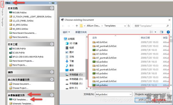
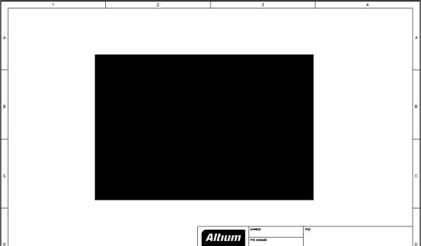
2) Select the preferred layout documents and also click the "Open" switch to produce a PCB document with an attractive infobox, as revealed listed below.
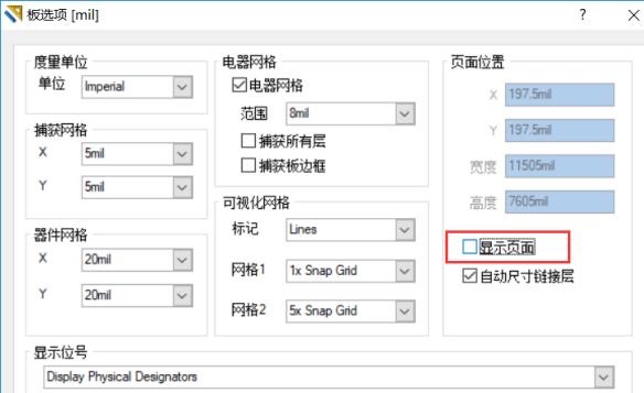
3) If the individual does not desire a white web page of the PCB data, you can carry out the food selection bar command "Style" → "Board specification alternative" or perform the faster way trick "DO", in the board choice will certainly be" The choice to present the web page is untreated, as revealed listed below.
( 4) Customers can double-click any type of thing in the info box to open up the edit dialog box to get in the equivalent details, as well as additionally include or remove the infobox web content.
( 1) Open up a PCB theme, choose the attractive details you require, and afterward do the duplicate procedure.
( 2) Change to the PCB documents that require to include attracting info, established the ideal illustration dimension, and afterward, do the paste procedure, as well as choose the ideal placement to put the formerly duplicated attracting details.
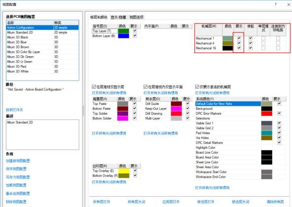
( 3) Customers require to be able to choose whether to present attracting details via the layer screen setups. Carry out the faster way essential L, embedded in the "Sight Options", as revealed listed below:
( 4) The attractive details pasted can additionally be changed. Mount the technique explained over to establish it.
Still, need help? Contact Us: support@nextpcb.com
Need a PCB or PCBA quote? Quote now


 Surface

