
 Surface


Julia Wu - Senior Sales Engineer at NextPCB.com

 NextPCB Capabilities
Printed Circuit Boards
NextPCB Capabilities
Printed Circuit Boards
 PCB Assembly
 Layer Buildup
 SMD-Stencils
 PCB Design-Aid & Layout
 Mechanics
 Quality
 Drills & Throughplating
 Factory & Certificate
 PCB Assembly Factory Show
Certificate
PCB Assembly Factory Show
Certificate
Support Team
Feedback:
support@nextpcb.com


The MLCC—Multilayer Ceramic Capacitor—is the most manufactured electronic component on earth. Murata alone produces approximately one trillion MLCCs per year. A single flagship smartphone contains over 1,000 of them. A modern AI server baseboard carries 40,000 to 60,000 MLCCs across its power delivery network, signal conditioning circuits, and EMI filters. Yet despite their ubiquity, MLCCs are frequently misapplied: wrong dielectric type, wrong package size, insufficient voltage rating, or incorrect placement—any of which can cause circuit instability, excessive noise, or premature failure.
This guide covers everything a PCB engineer needs to select and apply MLCCs correctly: internal construction, dielectric classification, package size trade-offs, ESR/ESL behavior, voltage derating, piezoelectric effects, placement rules, and a practical selection framework organized by application type.
An MLCC (Multilayer Ceramic Capacitor) is a surface-mount passive component that stores electrical charge using a ceramic dielectric material sandwiched between multiple thin conductive electrode layers. The “multilayer” in the name refers to the stacked internal structure: dozens to hundreds of alternating ceramic and metal electrode layers are co-fired into a monolithic block, then terminated with metal end caps that connect to the PCB pads via solder.
MLCCs are non-polarized—they can be placed in either orientation on the PCB, unlike electrolytic or tantalum capacitors which have a defined positive terminal. They are available in capacitance values from 0.1 pF to 100 μF (and beyond in newer high-capacitance grades), voltage ratings from 4 V to 10,000 V, and package sizes from 008004 (0.25 mm × 0.125 mm, smaller than a grain of salt) to 8060 (20.3 mm × 15.2 mm for high-voltage applications).
The ceramic dielectric material determines the MLCC's electrical behavior far more than the capacitance value stamped on the reel: two 100 nF capacitors in the same 0402 package from the same manufacturer can behave completely differently depending on whether they use C0G or X7R dielectric. Understanding this distinction is the most important MLCC knowledge any PCB engineer can have.
An MLCC is constructed through a ceramic tape casting and co-firing process:
The capacitance value is determined by: C = εr × ε0 × A × n / d, where εr is the relative permittivity of the ceramic, A is the electrode overlap area, n is the number of active layers, and d is the dielectric layer thickness. Increasing layer count (n) and reducing layer thickness (d) are the primary manufacturing levers for achieving higher capacitance in smaller packages—which is why modern 0402 MLCCs achieve capacitances that required 1206 packages a decade ago.
The EIA (Electronic Industries Alliance) classifies ceramic capacitor dielectrics into two broad categories with very different performance characteristics:
Class I (Temperature Compensating): Uses paraelectric ceramic compositions (typically calcium titanate + additives) with very stable, predictable capacitance versus temperature, voltage, and frequency. The dielectric constant (εr) is relatively low (6–200), limiting capacitance density, but the stability is excellent. Suitable for precision timing, filtering, and RF circuits where capacitance predictability is essential.
Class II (High Capacitance): Uses ferroelectric ceramic compositions (barium titanate-based) with very high dielectric constants (εr = 1,000–20,000+) that enable high capacitance in small packages. The trade-off is that capacitance varies significantly with temperature, applied DC voltage, AC voltage level, frequency, and age. Essential for general decoupling, bulk energy storage, and filtering applications where absolute capacitance stability is less critical than capacitance density.
C0G (read “C zero G”) and NP0 (negative-positive zero) are the most important Class I dielectrics. They are functionally identical: C0G is the EIA designation, NP0 is the older IEC/industry designation. Both describe a ceramic composition with:
C0G capacitors are the correct choice for:
Other Class I codes exist for different temperature coefficient slopes: P2G (−150 ppm/°C ± 60 ppm/°C, used for temperature compensation), N750 (−750 ppm/°C, used in specific RF tank circuit applications), etc. For most PCB design purposes, C0G/NP0 is the only Class I dielectric engineers need to specify regularly.
Class II dielectrics use the EIA three-character code system: the first character is the lower operating temperature limit, the second is the upper limit, and the third is the maximum capacitance change over that range.
X7R (most widely used Class II):
X5R:
Y5V (avoid for most applications):
X6S and X7S: Newer Class II codes with tighter tolerances (±22% and ±22% respectively) and better DC bias behavior than X7R in some compositions, increasingly used in automotive and industrial designs requiring better stability than standard X7R.
| Property | C0G / NP0 | X7R | X5R | Y5V |
|---|---|---|---|---|
| Temperature range | −55°C to +125°C | −55°C to +125°C | −55°C to +85°C | −30°C to +85°C |
| Capacitance change (temp) | ± 30 ppm/°C | ± 15% | ± 15% | +22% / −82% |
| DC bias effect | None measurable | Significant (−50% at half rated V typical) | Significant (−50% at half rated V typical) | Severe (−80% possible) |
| Aging effect | None | ~2–5% per decade | ~2–5% per decade | ~7–10% per decade |
| Loss factor (tan δ) | < 0.001 at 1 MHz | ~0.020–0.035 at 1 MHz | ~0.020–0.035 at 1 MHz | ~0.050+ at 1 MHz |
| Piezoelectric effect | None (paraelectric) | Present (ferroelectric) | Present (ferroelectric) | Strong |
| Maximum capacitance (0402) | ~100 nF | ~10 μF | ~22 μF | ~10 μF |
| Maximum capacitance (1210) | ~470 nF | ~100 μF | ~220 μF | ~220 μF |
| Typical applications | RF, precision timing, PLL, ADC reference | General decoupling, filtering, signal coupling | High-capacitance decoupling, consumer electronics | Non-critical AC filtering only |
| IEC / EIA Class | Class I (temperature compensating) | Class II (high capacitance) | Class II (high capacitance) | Class II (high capacitance) |
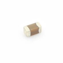
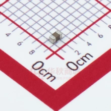
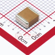
MLCC package sizes are designated by a four-digit EIA code where the first two digits give the length and the second two digits give the width in hundredths of an inch. A 0402 component is 0.04 inches (1.0 mm) long and 0.02 inches (0.5 mm) wide.
| EIA Code | Metric Code | Length × Width (mm) | Typical Max Capacitance | Assembly Notes |
|---|---|---|---|---|
| 008004 | 0201M | 0.25 × 0.125 | ~10 nF | Requires specialized high-precision SMT equipment; near-limit of manual rework capability |
| 0201 | 0603M | 0.60 × 0.30 | ~100 nF | Requires pick-and-place with vision alignment; very high placement density possible |
| 0402 | 1005M | 1.0 × 0.5 | ~22 μF (X5R) | Most common size for decoupling in high-density PCBs; standard SMT equipment handles without issue |
| 0603 | 1608M | 1.6 × 0.8 | ~47 μF (X5R) | Standard size for moderate-density designs; easier manual rework than 0402 |
| 0805 | 2012M | 2.0 × 1.25 | ~100 μF (X5R) | Used for bulk capacitance; available in higher voltage ratings for power circuits |
| 1206 | 3216M | 3.2 × 1.6 | ~100 μF | High capacitance or high voltage; larger thermal mass can affect reflow profile |
| 1210 | 3225M | 3.2 × 2.5 | ~220 μF | Bulk energy storage; significant piezoelectric noise risk in large X7R/X5R values |
| 2220 | 5750M | 5.7 × 5.0 | ~1,000 μF (specialty) | High-voltage, high-capacitance specialty types; very limited soldering window |
The trend toward smaller package sizes is driven by PCB density requirements. Modern AI server boards, as discussed in the context of GPU power delivery networks, pack thousands of 0201 and 0402 MLCCs in tight arrays around GPU package power delivery pins. Assembling 0201 components reliably requires pick-and-place machines with vision-based alignment, stencil apertures designed for the smaller pad geometry, and reflow profiles optimized for the reduced thermal mass. The SMT assembly considerations for these sizes are covered in depth in NextPCB's PCBA service.
A real-world MLCC is not a perfect capacitor. It has two parasitic impedance components that determine its performance at high frequencies:
ESR (Equivalent Series Resistance): The total resistive losses in the capacitor, including electrode resistance, termination contact resistance, and dielectric losses. ESR is the dominant dissipation mechanism in the capacitor and determines how much heat it generates under ripple current. ESR increases with frequency above the self-resonant frequency due to skin effect. For power supply decoupling, lower ESR is generally better; for some damping applications (like input filter stabilization in switching converters), a specific ESR value may be required.
ESL (Equivalent Series Inductance): The parasitic inductance of the capacitor's internal electrodes and termination connections. ESL is the primary factor limiting the capacitor's effectiveness at high frequencies. At the self-resonant frequency (SRF), the capacitor's reactance equals the inductive reactance: SRF = 1 / (2π × √(L × C)). Above the SRF, the component behaves as an inductor, not a capacitor—it no longer provides a low-impedance path to ground for high-frequency noise.
Key relationships between package size and ESL:
The three-tier decoupling strategy used in high-speed PCB design (bulk + mid-frequency + high-frequency capacitors) is fundamentally a strategy for managing the ESR/ESL behavior of MLCCs: bulk electrolytic capacitors handle low-frequency transients where MLCCs would need impractically large values; multiple 10–100 nF X7R MLCCs handle mid-frequency decoupling; multiple 1–10 nF C0G MLCCs handle high-frequency decoupling above the SRF of the X7R capacitors.
The most dangerous MLCC selection mistake is ignoring the DC bias effect in Class II dielectrics. Because X7R, X5R, and similar ferroelectric ceramics are piezoelectric materials, their dielectric constant decreases when an electric field is applied (this is the electrostriction / reverse piezoelectric effect manifesting as the DC bias effect).
The magnitude of this effect is dramatic and often underappreciated:
This means a decoupling capacitor placed on a 5 V power rail using a 10 V rated X7R MLCC delivers far less than its marked capacitance. Engineers who select MLCCs based on nominal capacitance value without accounting for the DC bias effect will find their actual power supply impedance to be several times higher than calculated.
Practical derating rules:
Class II MLCCs (X7R, X5R, Y5V) use ferroelectric barium titanate ceramic, which is piezoelectric: it physically deforms in response to an applied electric field. When an AC voltage is applied to an X7R MLCC—such as the AC ripple on a switching power supply output—the capacitor physically vibrates at the ripple frequency. If that frequency falls in the audible range (20 Hz–20 kHz), the PCB acts as a speaker diaphragm and the capacitor generates acoustic noise.
This effect is common in switch-mode power supplies, LED drivers, and motor control circuits where the switching frequency or a harmonic falls in the audible band. The mechanical stress from the vibration can also cause solder joint fatigue over time.
Mitigation strategies:
| Application | Recommended Dielectric | Recommended Package | Key Specification Notes |
|---|---|---|---|
| Crystal oscillator load capacitors | C0G / NP0 | 0402 or 0603 | Match capacitance to crystal spec; use ±1% or ±2% tolerance for frequency accuracy |
| RF bypass / blocking (50 Ω systems) | C0G / NP0 | 0402 or 0201 | Check SRF; use high-Q MLCC variants; NPO-RF series from Murata/AVX preferred |
| PLL supply bypass | C0G / NP0 | 0402 | Avoid X7R to prevent piezoelectric noise coupling into VCO; use C0G 100 nF + C0G 10 nF in parallel |
| ADC / DAC reference filter | C0G / NP0 | 0402 or 0603 | Capacitance stability directly affects conversion accuracy; C0G is mandatory |
| General IC power decoupling (1.0–5.0 V) | X7R | 0402 or 0201 | Use 100 nF per power pin as starting point; derate voltage 2×–3× supply; verify actual C at bias |
| Bulk bypassing on supply rail | X7R or X5R | 0805 or 1206 | 10 μF–100 μF; account for DC bias derating; verify C at operating voltage |
| GPU / CPU PDN decoupling (AI server) | X7R | 0201 or 0402 | High-density arrays; 100 nF in 0201 for mid-frequency; 1–10 μF in 0402 for bulk; verify via anti-pad clearances won't disrupt reference planes |
| EMI filter / input filter (power stage) | X7R or X5R | 1206 or 1210 | Consider piezoelectric noise at switching frequency; soft termination MLCCs reduce crack risk in high-vibration environments |
| High-voltage applications (> 100 V) | X7R (high-voltage grade) | 0805–2220 | Murata HV series, TDK HV series; safety-rated MLCCs (Y1, Y2, X1, X2 classes) for line-referenced applications |
| Automotive power supply decoupling | X7R (AEC-Q200 qualified) | 0402–1206 | AEC-Q200 qualification required; consider X8R or X7S for higher stability; 125°C or 150°C Tmax depending on placement zone |
| AC coupling (signal path) | C0G / NP0 for precision; X7R for general | 0402 or 0603 | Capacitance drift in X7R can shift AC cutoff frequency; use C0G where bandwidth consistency matters |
Correct MLCC selection is only half the equation—placement and PCB layout determine whether the selected capacitor actually delivers its intended function.
Rule 1: Place decoupling capacitors as close as possible to the power pin they serve. The effectiveness of a decoupling capacitor decreases with distance because the PCB trace between the capacitor and the IC's power pin adds inductance in series with the capacitor. Every millimeter of trace adds approximately 0.5–1 nH of inductance, which raises the impedance of the decoupling network at high frequencies. The capacitor should be on the same side of the PCB as the IC, with the shortest possible trace path from capacitor pad to IC power pad.
Rule 2: Connect to the power via first, not the IC pin first. Route the decoupling capacitor so that current flows from the power plane through the capacitor and then to the IC power pin, not the other way around. This ensures that the capacitor's charge reservoir is between the power plane and the IC, minimizing the inductance in the critical current path.
Rule 3: Use via-in-pad for the tightest placements. On high-density PCBs where 0201 or 0402 capacitors must be placed immediately adjacent to fine-pitch BGA power pins, via-in-pad (VIPPO) structures allow the capacitor pad to directly connect to the power plane through the pad, eliminating trace length entirely.
Rule 4: Multiple small capacitors outperform one large capacitor. Placing four 100 nF capacitors around an IC provides lower effective impedance than one 400 nF capacitor, because the four capacitors have quarter the ESL in parallel and provide decoupling from four different directions around the IC.
Rule 5: Orient MLCC long axis parallel to current flow. The internal electrodes of an MLCC run parallel to the long axis of the package. Orienting the capacitor with its long axis parallel to the current flow direction from via to IC minimizes the parasitic inductance of the PCB trace segment.
Rule 6: Avoid placing large (1206+) MLCCs near mechanical stress points. MLCCs are ceramic and can crack from PCB flexure. The risk is highest for large packages placed near PCB edge connectors, mounting holes, or depanelization routes. For mechanically stressed areas, use soft-termination MLCCs or shift to polymer capacitors.
Rule 7: Separate C0G and X7R capacitors on sensitive supply rails. If both C0G and X7R capacitors are required on the same supply node (for example, a 100 nF C0G for high-frequency bypassing and a 10 μF X7R for bulk decoupling), separate them by a small series ferrite bead or resistance to prevent the X7R's piezoelectric noise from coupling into the C0G's bypass path.
The MLCC market is dominated by a small number of Japanese and Korean manufacturers:
For production programs, sourcing MLCCs from multiple qualified manufacturers (cross-qualification) reduces supply chain risk. During the 2018–2019 MLCC shortage and the emerging 2026 tightness in high-capacitance grades, engineers who had qualified second sources experienced far less production disruption than those single-sourced to one manufacturer.
In actual PCB design and component procurement, choosing the right part number is crucial. To help engineers apply the selection rules discussed earlier, we have highlighted several highly representative ceramic capacitors (including SMD MLCCs and through-hole monolithic capacitors) for various applications. These cover common long-tail requirements ranging from micro 0201 packages to large 2220 sizes:
| Part Number | Manufacturer | Package Size | Dielectric | Capacitance | Voltage | Key Characteristics & Applications |
|---|---|---|---|---|---|---|
| GRM0335C1H2R4CA01D | Murata | 0201 (0603M) | C0G (NP0) | 2.4 pF | 50V | High frequency, high stability. Ultra-small package suitable for precision circuits with strict parasitic inductance requirements, such as RF matching and crystal oscillator loads. |
| TCC0603X7R102M500CT | CCTC | 0603 (1608M) | X7R | 1 nF | 50V | Cost-effective general-purpose SMD capacitor. Ideal for standard IC signal decoupling and mid-frequency filtering networks. |
| FS55X106K500EHG | PSA | 2220 (5750M) | X7R | 10 μF | 50V | Large size, high capacitance. Capable of handling higher voltage derating requirements, making it perfect for main power rail bulk energy storage and low-frequency bypassing. |
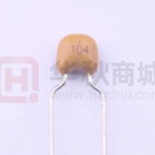
| 05B104K500PF3C1N0R | STE | Through-Hole (P=5.08mm) | X7R | 100 nF | 50V | Leaded radial monolithic capacitor with excellent resistance to mechanical stress. Suitable for wave soldering processes, power boards, or specific through-hole PCB designs. |
Note: Before adding these components to your BOM or PCB layout, please verify your actual operating voltage and refer back to the "Voltage Derating" rules mentioned earlier. This ensures the effective capacitance in your live circuit meets your design requirements.
What does MLCC stand for?
MLCC stands for Multilayer Ceramic Capacitor. The “multilayer” refers to the internal construction: hundreds of alternating ceramic dielectric layers and metal electrode layers are co-fired into a single monolithic chip, creating the high capacitance-to-volume ratio that makes MLCCs the most widely used capacitor type in electronics.
What is the difference between C0G and X7R?
C0G (also called NP0) is a Class I dielectric with near-zero temperature coefficient, no DC bias effect, and no aging. It is the most stable MLCC type but limited to lower capacitance values. X7R is a Class II dielectric with much higher dielectric constant (enabling more capacitance in the same package) but with ±15% capacitance variation with temperature, significant capacitance loss under DC bias (50–80% at half rated voltage is common), and a piezoelectric effect. Use C0G wherever stability matters (oscillators, PLL, RF, precision circuits); use X7R for general-purpose decoupling where high capacitance density is the priority.
Why does my MLCC measure much less capacitance than its marked value?
If you are measuring a Class II (X7R, X5R) MLCC on a live circuit or with DC bias applied, the DC bias effect is almost certainly the cause. Barium titanate-based ceramics lose 50–90% of their capacitance when an electric field is applied, depending on the ratio of applied voltage to rated voltage. To measure true capacitance, remove the capacitor from the circuit and measure at zero bias, or use the manufacturer's DC bias characteristic curves to calculate effective capacitance at your operating voltage.
Can I replace an electrolytic capacitor with an MLCC?
For capacitance values up to approximately 100 μF, modern MLCCs can replace electrolytic capacitors in many applications. MLCCs have lower ESR and better high-frequency performance, longer operating life (no liquid electrolyte to dry out), smaller size, and no polarity constraint. However, for bulk storage requirements above 100 μF, or in applications requiring voltage-variable capacitance (unlikely to be desirable), electrolytic or polymer capacitors remain necessary. Always verify that the MLCC's actual capacitance under DC bias (for Class II types) meets the minimum required for the specific application.
How many MLCCs does a GPU server board actually use?
A modern AI server GPU baseboard (such as an H100 or B200 DGX baseboard) uses between 40,000 and 60,000 MLCCs per board. The majority are small (0201 or 0402) X7R capacitors in the 100 nF to 10 μF range, used in dense arrays around each GPU and NVSwitch package for power delivery decoupling. A smaller number of C0G capacitors are used in timing-critical and signal conditioning circuits. The total passive component population of a modern AI cluster rack can exceed several million MLCCs.
What is the shelf life of an MLCC?
MLCCs have no inherent shelf life limit when stored properly (dry, room temperature, in original sealed packaging). However, the solderability of the termination finish degrades over time due to oxidation, particularly for standard tin-over-nickel finishes. IPC J-STD-020 defines MSL (Moisture Sensitivity Levels) for MLCCs, but standard MLCCs are typically rated MSL 1 (unlimited floor life at ≤ 30°C / 85% RH). Reels stored beyond 2 years in non-controlled environments may require reflow testing before use in production to verify solderability.
Whether your design uses thousands of 0201 MLCCs around a GPU power delivery network or precision C0G capacitors in a high-frequency RF circuit, NextPCB provides the SMT assembly precision, solder paste inspection, and quality control processes to assemble passive components correctly—from standard 0402 MLCCs through the most demanding 0201 high-density arrays.
Get a PCBA quote from NextPCB →
For high-layer-count PCBs where MLCC decoupling via placement requires via-in-pad or HDI technology, explore NextPCB's HDI PCB capabilities.

Still, need help? Contact Us: support@nextpcb.com
Need a PCB or PCBA quote? Quote now

