

 NextPCB Capabilities
 PCB Assembly
 Layer Buildup
 SMD-Stencils
 PCB Design-Aid & Layout
 Mechanics
 Surface
 Quality
 Drills & Throughplating
 Factory & Certificate


In this guide, you will learn:
- What ODB++ is (and why it is not just "another format")
- How ODB++ compares to legacy Gerber file workflows
- Which tools to use for Gerber viewer vs. ODB++ viewer tasks
- Where IPC-2581 fits in the future of digital manufacturing
If you are still exporting separate Gerber file layers and a separate drill file, you are leaving money on the table. Let's fix that.
1. What is ODB++? (And Why Should You Care?)
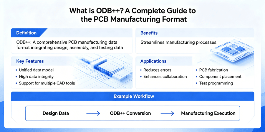
ODB++ (Open Database ++) was originally developed by Valor Computerized Systems (now part of Siemens EDA). Unlike a traditional Gerber file — which describes images layer by layer — ODB++ describes the intent of the design.
What ODB++ Contains
| Data Type | Gerber | ODB++ |
|---|---|---|
| Copper imagery | Yes (one file per layer) | Yes (integrated) |
| Soldermask & silkscreen | Yes | Yes |
| Drill data | Separate Excellon file | Embedded |
| Netlist (connectivity) | No (separate IPC netlist) | Yes |
| Component placement | No | Yes (centroid & rotation) |
| Impedance stackup | No | Yes |
| Fabrication notes | Separate readme.txt | Embedded in XML |
Because ODB++ is a single database (actually a folder structure with multiple files), the CAM engineer at your fab house imports one thing — not 20+ separate files that might be misaligned or missing.
The "Single Source of Truth" Advantage
With Gerber file output, every revision carries risk:
- Did you regenerate all layers after moving a via?
- Is the drill file still aligned with the copper?
- Did the soldermask expansion change?
With ODB++, the CAM system rebuilds the entire PCB from the database. Alignment is automatic. Layers cannot drift. It is, simply, a more robust handoff.
2. ODB++ vs. Gerber Comparison
The modern Gerber file format (RS-274X) is actually very good — for a vector image format. But PCB manufacturing is not image processing; it is fabrication.
The Layer Alignment Problem
Consider an 8-layer board with buried vias and blind microvias. To export Gerber file data correctly, you must generate:
- 8 copper layers
- 2 soldermask layers (top/bottom)
- 2 silkscreen layers
- 4 drill files (one for each unique via type)
- 1 IPC-D-356 netlist
That is 17 separate files. If any single file is from an outdated revision, the board fails. If the drill files use different coordinate origins, holes will be offset. These are real, everyday failures.
ODB++ eliminates this entirely. One export. One folder. One revision.
Data Density & HDI
For HDI boards with 50µm lines and laser-drilled microvias, floating-point precision matters. ODB++ uses double-precision arithmetic internally. Standard Gerber file coordinates, even with extended X2 attributes, are still limited. When you see "Gerber-to-ODB++ translation errors" in CAM, that is often the culprit.
Netlist Verification with an ODB++ viewer
This is the killer feature: netlist awareness.
- With a Gerber viewer, you can see a pad. But you cannot click on it and ask, "What net is this?" Because Gerber contains no connectivity data.
- With an ODB++ viewer, you click any pad and instantly see the net name (e.g., "DDR4_DQ31"), component reference, and pin number.
For DFM review, that is night and day. You can spot an unconnected thermal pad or a shorted differential pair before the CM does.
One Tool, All Formats: Gerber, ODB++, & KiCad files
3. The PCB File Viewer: Gerber viewer vs. ODB++ viewer
You will always need both types of tools. Here is when to use each.
When to use a Gerber viewer
Free Gerber viewer tools (like HQDFM, Gerbv, GC-Prevue, or Kicad viewers) are great for:
- Quick layer visibility checks
- Measuring a pad or trace distance
- Checking that the soldermask does not cover a gold finger
But a Gerber viewer cannot tell you if the netlist matches the layout. It cannot confirm polarity of a diode. It is a picture viewer — powerful, but limited.
When to use an ODB++ viewer
A dedicated ODB++ viewer (free options include the Ucamco Reference Viewer, HQDFM and Siemens Valor NPI viewer) adds:
- Netlist probing (click a pad → see the net)
- Component browsing (see all R0402 resistors, their positions, and their net connections)
- Layer stackup verification (material, thickness, impedance)
- Gap & clearance checking with electrical context
Try Gerber Viewer & ODB++ Viewer Online
4. IPC-2581: The Open Standard Alternative
You cannot discuss ODB++ without mentioning IPC-2581. This is the only open, royalty-free, industry-standard format for PCB manufacturing data, developed by the IPC (Association Connecting Electronics Industries).
ODB++ vs. IPC-2581: Key Differences
| Feature | ODB++ | IPC-2581 |
|---|---|---|
| Ownership | Siemens EDA (proprietary) | IPC (open standard) |
| License | Royalty-free for read/write | Royalty-free |
| File structure | Directory of multiple files | Single XML file (.xml or .tgz) |
| Industry adoption | Very high (all major CMs) | Growing (defense/aerospace) |
| Industry 4.0 features | Good | Excellent (built for smart factories) |
Which one should you use?
- ODB++ is the safe choice today. Every major CM (from Asia to Europe to North America) accepts ODB++ without question. If you send ODB++, they will thank you.
- IPC-2581 is the future-proof choice. If you work on long-lifecycle military, aerospace, or automotive programs, contracts are increasingly specifying IPC-2581 because it is an open standard with no vendor lock-in.
Reality: Many engineers export ODB++ for production and IPC-2581 for long-term archiving. There is no law that says you must pick only one.
> Recommend reading: Gerber vs. ODB++ vs. IPC-2581: Do We Really Need Smarter PCB Formats
5. How to Generate ODB++ from Major EDA Tools
Here are step-by-step instructions for common tools.
Altium Designer
File → Fabrication Outputs → ODB++
Select "Separate folder" (not "Zipped file" — some CMs prefer unzipped)
Enable "Embedded netlist" and "Units: Metric"
Click "Configure" to set precision (10.6 is safe for most designs)
Generate
Cadence Allegro
Manufacture → ODB++ Inside
- Set output directory
- Choose "Units: Millimeter" and "Precision: 10.6"
- Under "Layers," verify all manufacturing layers are included (including soldermask, paste, silkscreen)
- Click "Translate"
KiCad
- Install the ODB++ plugin (Tools → External Plugins → ODB++)
- Select the output folder
- Use default settings (10.6 precision)
- Export
Mentor Xpedition
Output → Fabrication → ODB++
- Use the "Valor ODB++" option
- Run DFM Check before export
- Missing layers (e.g., top paste)
- Correct netlist (compare net count to your schematic)
- Stackup thickness (does it match your design?)
> Recommend reading: How to Export Gerber Files from Eagle/ KiCad/ Altium / Diptrace Software
6. Common Myths About ODB++
False. Small prototype houses also prefer ODB++ because it reduces their CAM engineering time. Less CAM time = lower NRE fees for you.
False. A Gerber file set plus separate drill files and netlist is often larger than an ODB++ folder. And size does not matter; correctness does.
False. A standard Gerber viewer cannot read ODB++. You need a dedicated ODB++ viewer (or your EDA tool's import feature). But you can export Gerbers from ODB++ if needed.
False. IPC-2581 is gaining ground, especially in open-source and military circles. But ODB++ remains the de facto standard for commercial PCB fabrication. Most CMs support both.
7. When to Stick with Gerber
Despite everything above, there are valid use cases for plain Gerber file output:
- Two-layer boards with <50 components — The risk of misalignment is very low.
- Legacy CMs — Some small, low-cost shops still use ancient CAM software that expects separate Gerber file layers. Ask first.
- Quick-turn prototype — If you are ordering from a fully automated online portal that only accepts Gerber+Excellon, just give them what they want.
But for anything with BGAs, impedance control, or >4 layers, ODB++ is the professional choice.
8. Conclusion: Make the Switch This Quarter
The Gerber file is not going away. It will continue to exist as a lowest-common-denominator format for PCB viewing and simple prototypes. But for manufacturing data release, ODB++ is objectively superior.
Your action plan:
- This week: Download a free ODB++ viewer (HQDFM, Ucamco Reference Viewer or Siemens Valor NPI Viewer).
- Next project: Export ODB++ instead of Gerber. Keep a Gerber viewer installed for quick checks, but use the ODB++ viewer for final verification.
- Ask your CM: "Do you prefer ODB++ or IPC-2581?" Their answer will tell you a lot about their technical maturity.
The days of "I forgot to include the drill file" are over. The days of "the soldermask shifted because I misaligned layers" are over. Export ODB++. Sleep better.
Frequently Asked Questions
A: Yes, some low-cost CMs still want separate Gerber file layers. Always ask in advance. But most mid-to-high tier CMs will accept it.
A: The format specification is royalty-free. You can read and write ODB++ without paying Siemens. EDA tool vendors may charge for their implementation, but that is separate.
A: Not yet, and probably not for years. Both will coexist. IPC-2581 is stronger for long-term archiving and open-source supply chains. ODB++ is stronger for immediate production.
A: The Ucamco Reference Viewer (Windows) is widely used. Siemens offers Valor NPI Viewer with more features but for limited time. For Linux users, some EDA tools can import ODB++ for viewing.
If you are looking for a powerful, free, and web-based solution that supports ODB++, Gerber (RS-274X/X2), and native KiCad files, highly recommend the NextPCB Gerber Viewer.

