
 NextPCB Capabilities
Printed Circuit Boards
NextPCB Capabilities
Printed Circuit Boards
 PCB Assembly
 Layer Buildup
 SMD-Stencils
 PCB Design-Aid & Layout
 Mechanics
 Quality
 Drills & Throughplating
 Factory & Certificate
 PCB Assembly Factory Show
Certificate
PCB Assembly Factory Show
Certificate
Support Team
Feedback:
support@nextpcb.com


With the widespread adoption of High-Density Interconnect (HDI) technology in electronic products, the design of Blind Vias and Buried Vias has become increasingly common in PCB Layout. Proper blind and buried via design not only effectively increases routing density but also optimizes signal return paths.
Before configuring via settings, engineers must first complete a rigorous stackup planning process. Parameters such as stackup thickness and dielectric constants directly determine the depth and impedance performance of the vias. It is recommended that during the early design phase, you use the NextPCB Impedance Calculator to evaluate trace width and layer spacing. For proven, manufacturable stackup solutions as a real-world design reference, you can consult the NextPCB Impedance Control Stackups.
This article uses a typical 8-layer board (1+6+1 HDI structure) as an example, featuring L1-L2 blind vias, L2-L7 buried vias, and L7-L8 blind vias. We will explore two mainstream methods for creating these blind and buried vias in Cadence Allegro.
The first method involves defining physical padstack files with specific start and end layers directly within the Pad Designer. This method features independent library files, making it easy to reuse them across different projects.
1. Creating L1-L2 Blind Vias
The specific stackup for this 8-layer board is shown in Figure 1. Open the "Pad_Designer" window and create a new file named "via10d4_l1-l2" (representing a 10mil outer diameter and 4mil inner diameter, from Layer 1 to Layer 2).
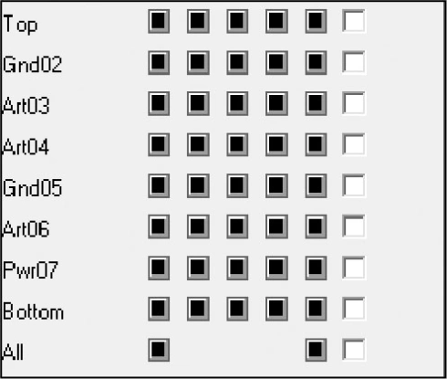
Figure 1: 8-layer PCB Stackup
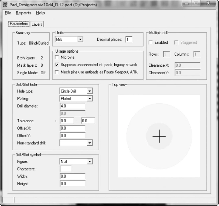
Figure 2: Parameters Tab Settings
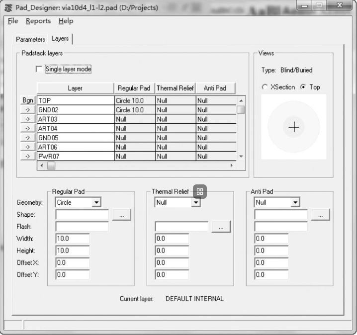
Figure 3: Layers Tab Settings - Part 1
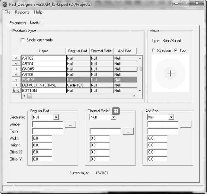
Figure 4: Layers Tab Settings - Part 2
2. Creating L2-L7 Buried Vias
Continue by creating a new file in Pad Designer named "via18d8_l2-l7".
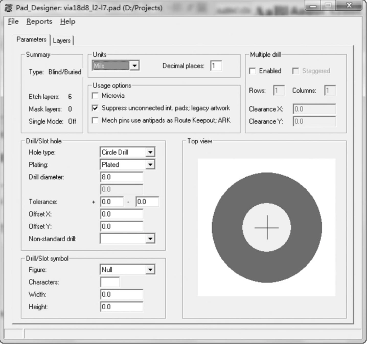
Figure 5: Parameters Tab Settings

Figure 6: Layers Tab Settings - Part 1
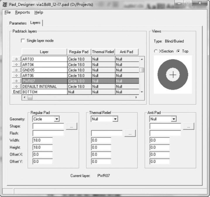
Figure 7: Layers Tab Settings - Part 2
3. Creating L7-L8 Blind Vias
Finally, create a new file named "via10d4_l7-l8".

Figure 8: Parameters Tab Settings
The second method involves creating standard through-hole padstacks first and then using system tools within the Allegro PCB Editor environment to define their span, effectively "transforming" them into blind or buried vias.
1. Prepare Standard Vias
Create two standard through-hole pads in Pad Designer, named "VIA10D4" and "VIA18D8".
2. Define Blind/Buried Via Attributes
After opening PCB Editor, go to the top menu and select Setup → B/B Via Definitions → Define B/B Via. Configure the popup window as shown in Figure 9.
The key parameter definitions in the window are as follows:
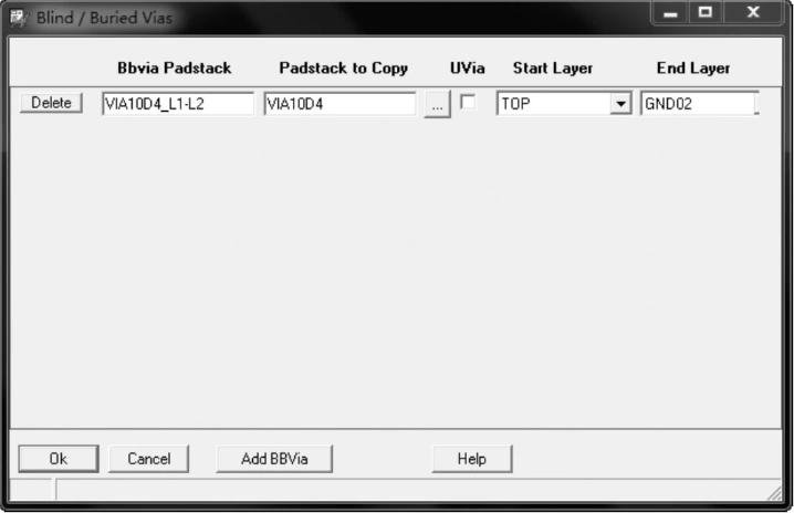
Figure 39: Define B/B Via Window Settings
3. Batch Add Remaining Vias
Click the "Add BBVia" button on the right side of the window to add the current definition to the list. Then, follow the same logic to create the buried via "VIA18D8_L2-L7" and the blind via "VIA10D4_L7-L8". The final configuration is shown in Figure 10.
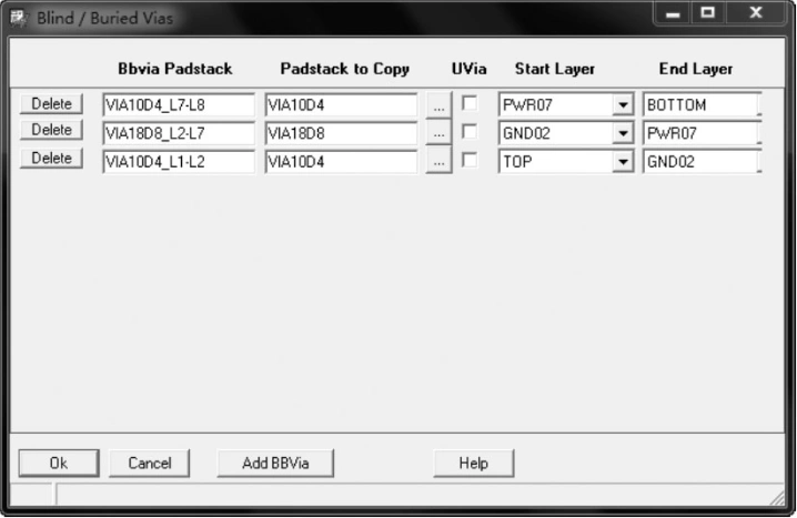
Figure 10: Completion of all Blind and Buried Via Definitions
4. Finalize Setup
After verifying the settings, click the "OK" button. The blind and buried vias for this PCB project are now created and ready to be called during routing.
In actual hardware engineering, both methods have their specific use cases:
Regardless of the method used, it is recommended that engineers design based on real-world stackup data provided by the manufacturer to ensure that the final Gerber files align with the factory's fabrication capabilities.
Avoid costly fabrication errors by NextPCB's Free DFM Check Service to verify your via-in-pad and stackup density before hitting the production line.
Still, need help? Contact Us: support@nextpcb.com
Need a PCB or PCBA quote? Quote now


 Surface

